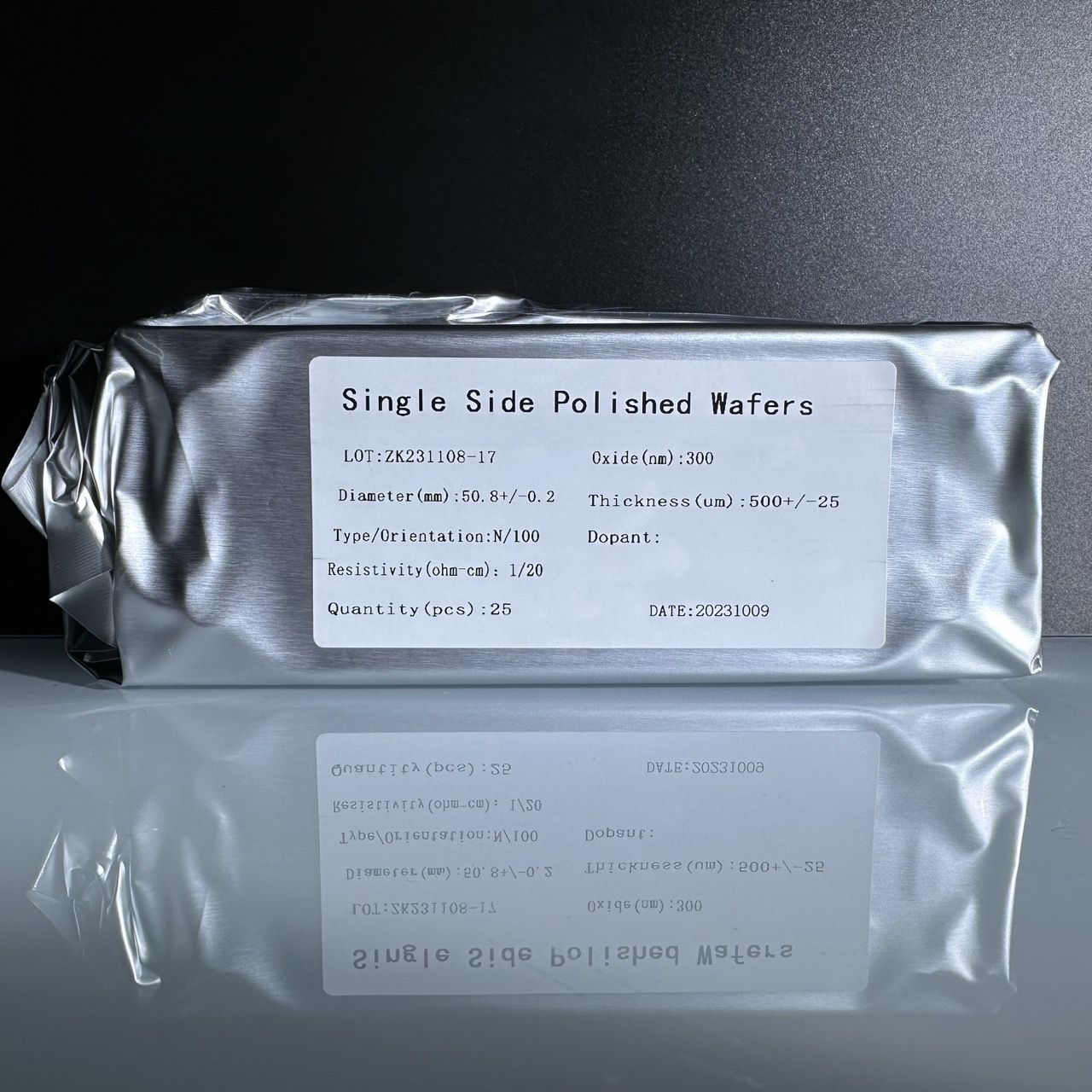
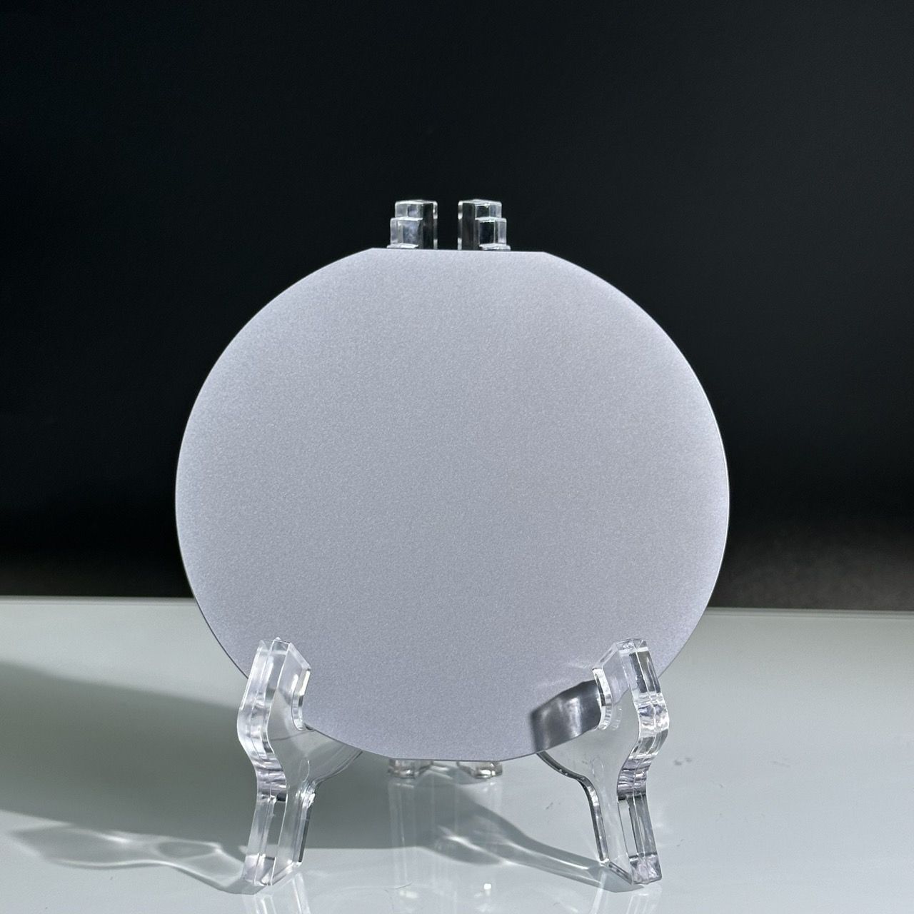
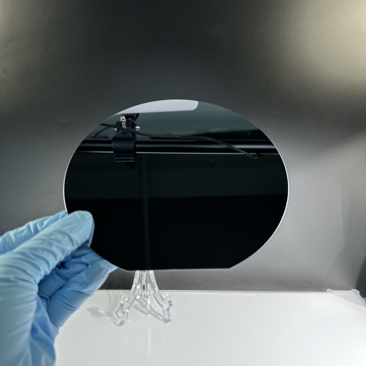
2inch 50.8mm Silicon wafer FZ N-Type SSP


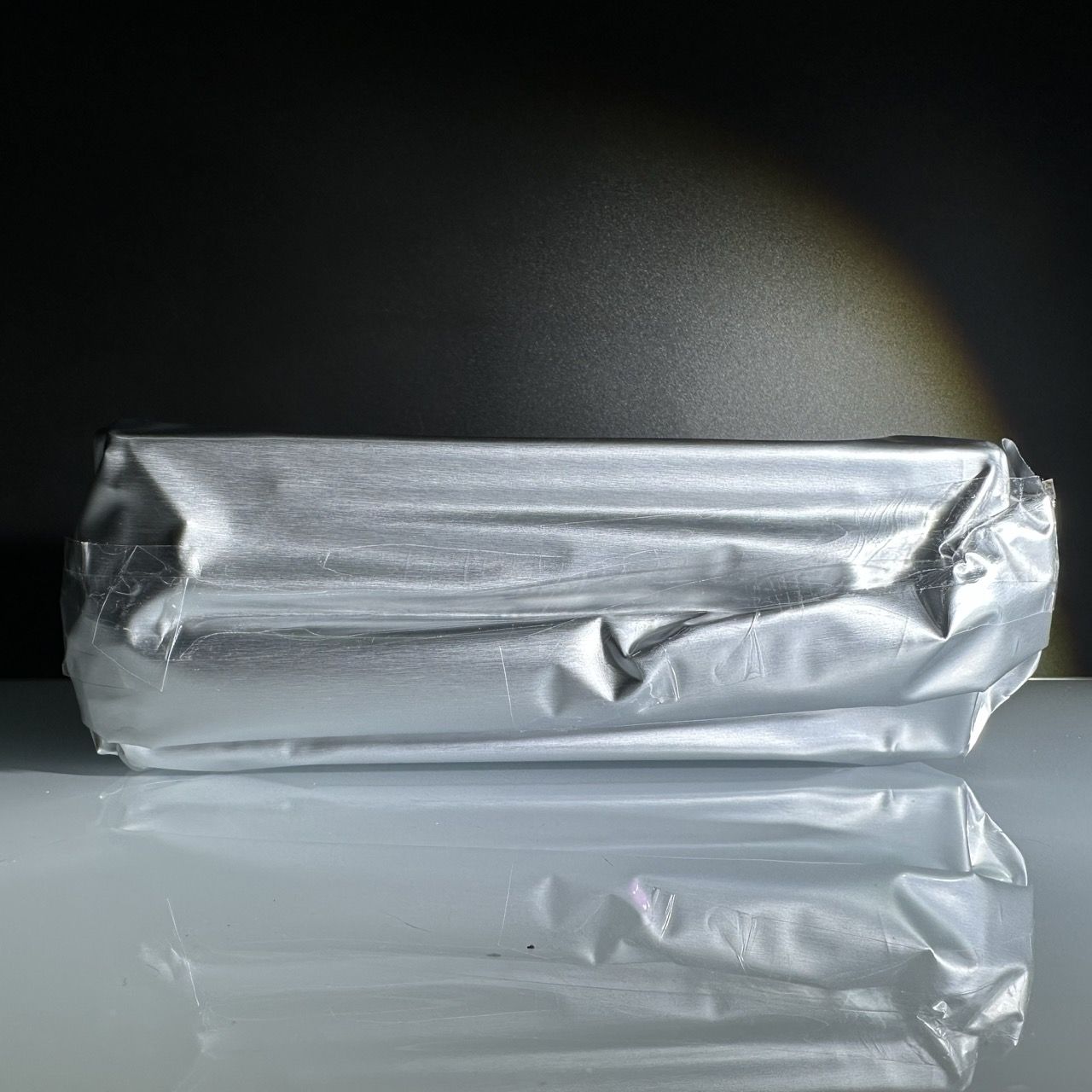
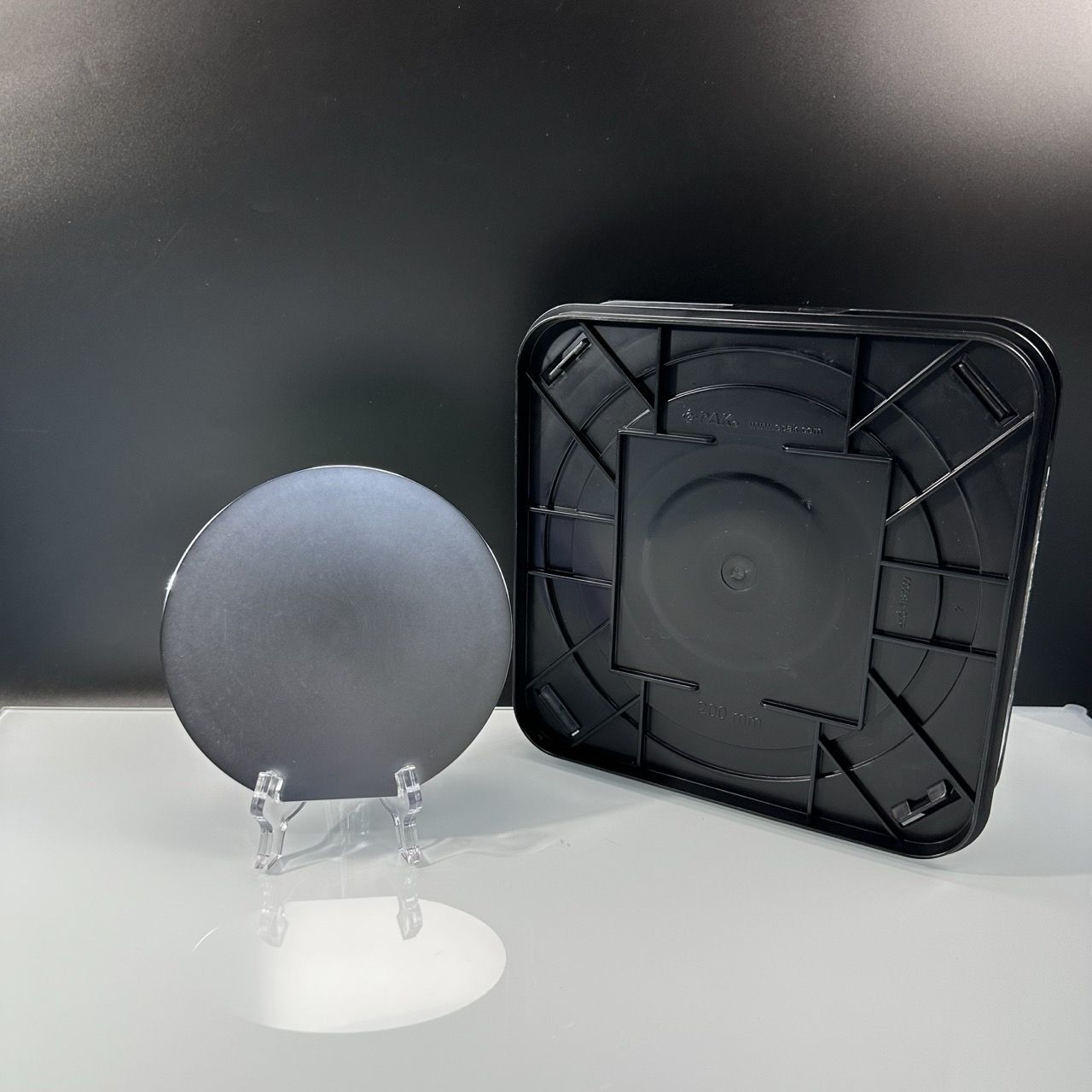
Introduce of wafer box
A 2-inch wafer is a smaller-sized silicon substrate that is commonly used to make microelectronic devices such as small integrated circuits and sensors. Its uses include, but are not limited to, micro sensors, micro actuators, and micro mechanical devices. Due to its small size, the commercial outlook is likely to be mainly in the microelectronics market as well as in sensor applications. In addition, with the development of IoT, wearable devices, and other fields, the demand for miniaturized and low-power electronic devices is likely to increase, which also brings commercial development opportunities for 2-inch silicon wafers.
| Silicon Wafer Technology: Wafer Size and Thickness | ||
| Thickness Range | Advantages | Considerations |
| Smaller Thickness | Improved thermal conductivity
Reduced warpage Compaction and miniaturization |
Reduced mechanical strength
Susceptibility to breakage |
| Larger Thickness | Enhanced mechanical integrity
Lower vulnerability to stress-induced defects |
Limited thermal conductivity
Increased warpage potential |
| 300 mm diameter | Industry-standard
Ideal productivity and cost |
Moderate susceptibility to defect |
| 450 mm diameter | Higher chip density per wafer
Increased productivity and cost efficieny |
Increased susceptibility to defect
Significant investment is required for equipment and infrastructure for a higher yield |
Although there are dozens of materials used to manufacture semiconductors, silicon is by far the most common. Silicon is not only easy to work with, but it is also so abundant that it presents the most cost-effective option.
Since silicon wafers have so many important uses and applications in everyday life, categorizing the most important ones can be a daunting task. Since silicon wafers are widely used and have many applications, it would be unfair to focus on only one of its applications. Here, we will focus on the applications and uses of silicon wafers in the field of electronic devices. If you want to learn more about the importance of silicon wafers in everyday life, read on.
The most popular semiconductor is silicon due to its high temperature and high mobility at room temperature, although other conductors have different uses in more specific applications. In electronic devices, it's a remarkable choice because current passes through silicon semiconductors more quickly than most conductors
Detailed Diagram