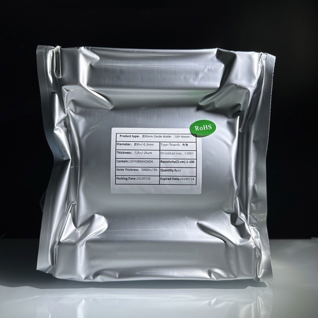
8inch Silicon wafer P/N-type (100) 1-100Ω dummy reclaim substrate
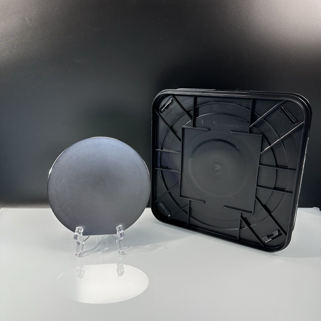

Introduce of wafer box
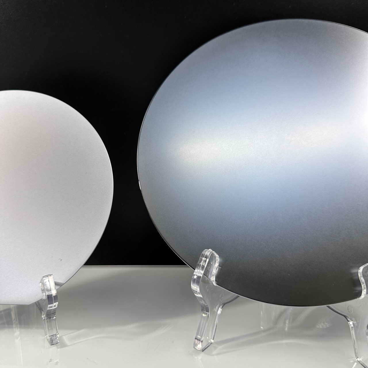
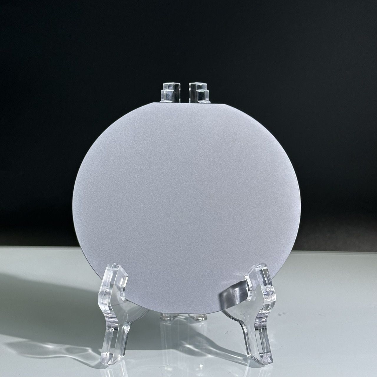
The 8-inch silicon wafer is a commonly used silicon substrate material and is widely used in the manufacturing process of integrated circuits. Such silicon wafers are commonly used to make various types of integrated circuits, including microprocessors, memory chips, sensors and other electronic devices. 8-inch silicon wafers are commonly used to make chips of relatively large sizes, with advantages including a larger surface area and the ability to make more chips on a single silicon wafer, leading to increased production efficiency. The 8-inch silicon wafer also has good mechanical and chemical properties, which is suitable for large-scale integrated circuit production.
Product features
8" P/N type, Polished silicon wafer (25 pcs)
Orientation: 200
Resistivity: 0.1 - 40 ohm•cm (It may vary from batch to batch)
Thickness: 725+/-20um
Prime/Monitor/Test Grade
MATERIAL PROPERTIES
| Parameter | Characteristic |
| Type/Dopant | P, Boron N, Phosphorous N, Antimony N, Arsenic |
| Orientations | <100>, <111> slice off orientations per customer's specifications |
| Oxygen Content | 1019 ppmA Custom tolerances per customer's specification |
| Carbon Content | < 0.6 ppmA |
MECHANICAL PROPERTIES
| Parameter | Prime | Monitor/ Test A | Test |
| Diameter | 200±0.2mm | 200 ± 0.2mm | 200 ± 0.5 mm |
| Thickness | 725±20µm (standard) | 725±25µm(standard) 450±25µm
625±25µm 1000±25µm 1300±25µm 1500±25 µm |
725±50µm (standard) |
| TTV | < 5 µm | < 10 µm | < 15 µm |
| Bow | < 30 µm | < 30 µm | < 50 µm |
| Wrap | < 30 µm | < 30 µm | < 50 µm |
| Edge Rounding | SEMI-STD | ||
| Marking | Primary SEMI-Flat only, SEMI-STD Flats Jeida Flat, Notch | ||
| Parameter | Prime | Monitor/ Test A | Test |
| Front Side Criteria | |||
| Surface condition | Chemical Mechanical Polished | Chemical Mechanical Polished | Chemical Mechanical Polished |
| Surface Roughness | < 2 A° | < 2 A° | < 2 A° |
| Contamination
Particles@ >0.3 µm |
= 20 | = 20 | = 30 |
| Haze,Pits
Orange peel |
None | None | None |
| Saw,Marks
Striations |
None | None | None |
| Back Side Criteria | |||
| Cracks, crowsfeet, saw marks,stains | None | None | None |
| Surface condition | Caustic etched | ||
Detailed Diagram