FZ CZ Si wafer in stock 12inch Silicon wafer Prime or Test


Introduce of wafer box
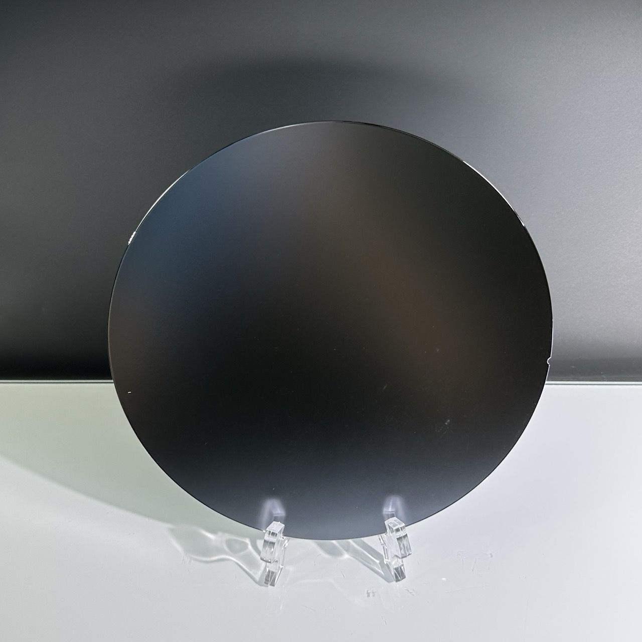
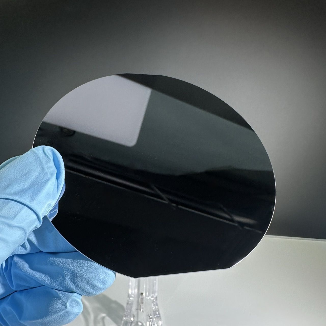
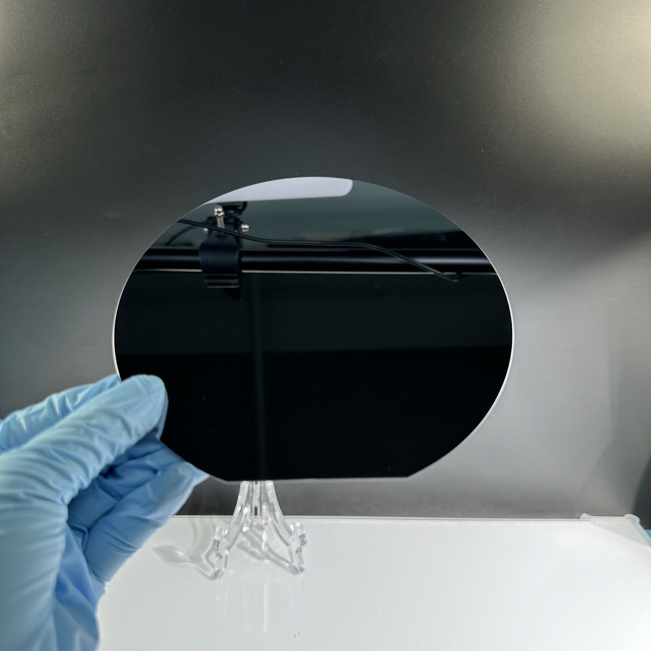
Polished Wafers
Silicon wafers that are specially polished on both sides to obtain a mirror surface. Superior characteristics such as purity and flatness define the best characteristics of this wafer.
Undoped Silicon Wafers
They are also known as intrinsic silicon wafers. This semiconductor is a pure crystalline form of silicon without the presence of any dopant throughout the wafer, thus making it an ideal and perfect semiconductor.
Doped Silicon Wafers
N-type and P-type are the two types of doped silicon wafers.
N-type doped silicon wafers contain arsenic or phosphorus. It is widely used in the manufacture of advanced CMOS devices.
Boron doped P-type silicon wafers. Mostly, it is used to make printed circuits or photolithography.
Epitaxial Wafers
Epitaxial wafers are conventional wafers used to obtain surface integrity. Epitaxial wafers are available in thick and thin wafers.
Multilayer epitaxial wafers and thick epitaxial wafers are also used to regulate energy consumption and power control of devices.
Thin epitaxial wafers are commonly used in superior MOS instruments.
SOI Wafers
These wafers are used to electrically insulate fine layers of single crystal silicon from the entire silicon wafer. SOI wafers are commonly used in silicon photonics and high performance RF applications. SOI wafers are also used to reduce parasitic device capacitance in microelectronic devices, which helps improve performance.
Why is wafer fabrication difficult?
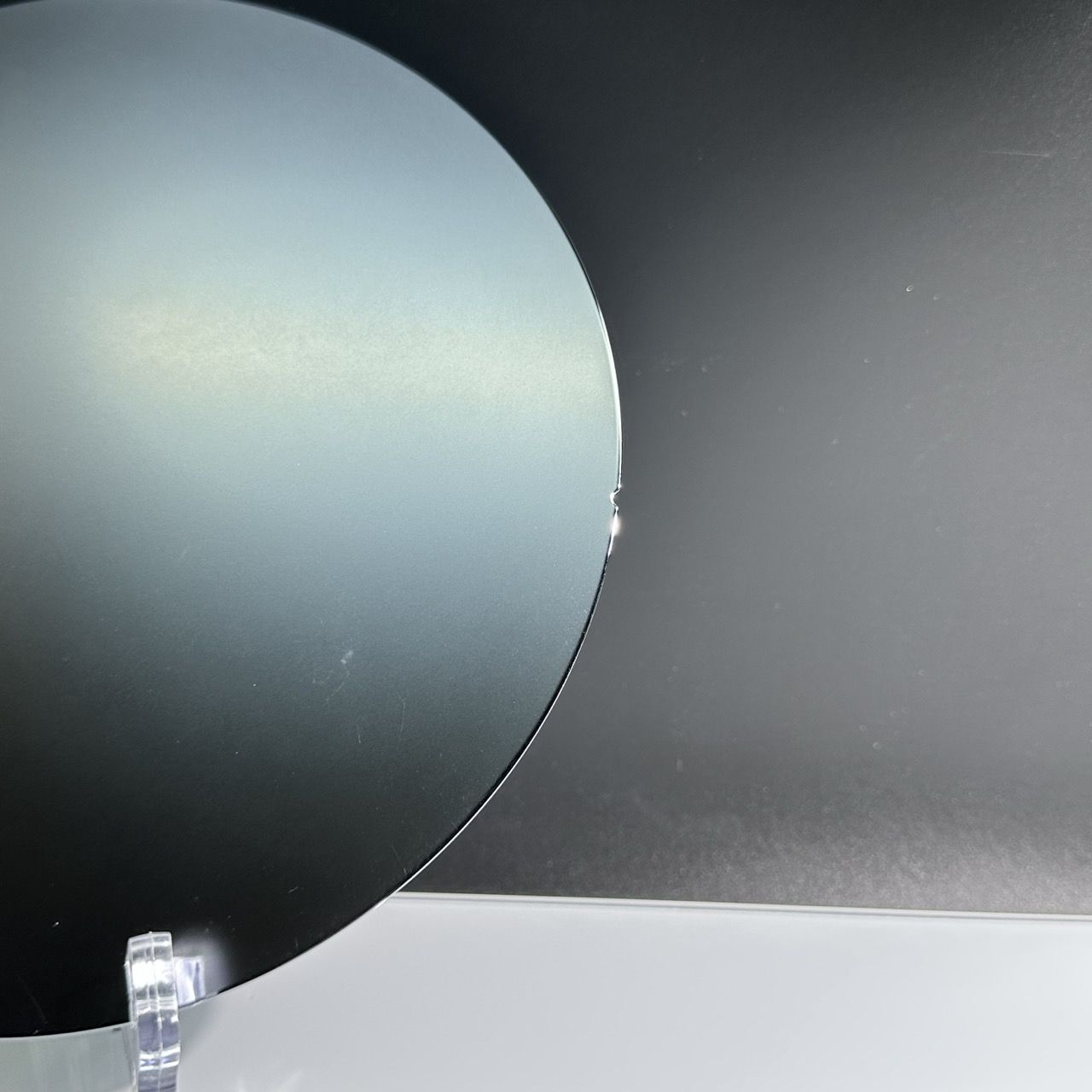
12-inch silicon wafers are very difficult to slice in terms of yield. Although silicon is hard, it is also brittle. Rough areas are created as sawn wafer edges tend to break. Diamond discs are used to smooth the wafer edges and remove any damage. After cutting, the wafers break easily because they now have sharp edges. Wafer edges are designed in such a way that fragile, sharp edges are eliminated and the chance of slippage is reduced. As a result of the edge forming operation, the diameter of the wafer is adjusted, the wafer is rounded (after slicing, the cut off wafer is oval), and notches or orientated planes are made or sized.
Detailed Diagram