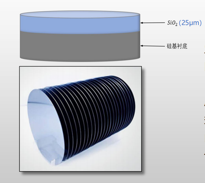
SiO2 Thin Film Thermal Oxide Silicon wafer 4inch 6inch 8inch 12inch

Introduce of wafer box
The main process of manufacturing oxidized silicon wafers usually includes the following steps: monocrystalline silicon growth, cutting into wafers, polishing, cleaning and oxidation.
Monocrystalline silicon growth: First, monocrystalline silicon is grown at high temperatures by methods such as the Czochralski method or the Float-zone method. This method enables the preparation of silicon single crystals with high purity and lattice integrity.
Dicing: The grown monocrystalline silicon is usually in a cylindrical shape and needs to be cut into thin wafers to be used as a wafer substrate. Cutting is usually done with a diamond cutter.
Polishing: The surface of the cut wafer may be uneven and requires chemical-mechanical polishing to obtain a smooth surface.
Cleaning: The polished wafer is cleaned to remove impurities and dust.
Oxidizing: Finally, the silicon wafers are put into a high-temperature furnace for oxidizing treatment to form a protective layer of silicon dioxide to improve its electrical properties and mechanical strength, as well as to serve as an insulating layer in integrated circuits.
The main uses of oxidized silicon wafers include the manufacture of integrated circuits, the manufacture of solar cells, and the manufacture of other electronic devices. Silicon oxide wafers are widely used in the field of semiconductor materials because of their excellent mechanical properties, dimensional and chemical stability, ability to operate at high temperatures and high pressures, as well as good insulating and optical properties.
Its advantages include a complete crystal structure, pure chemical composition, precise dimensions, good mechanical properties, etc. These features make silicon oxide wafers particularly suitable for the manufacture of high-performance integrated circuits and other microelectronic devices.
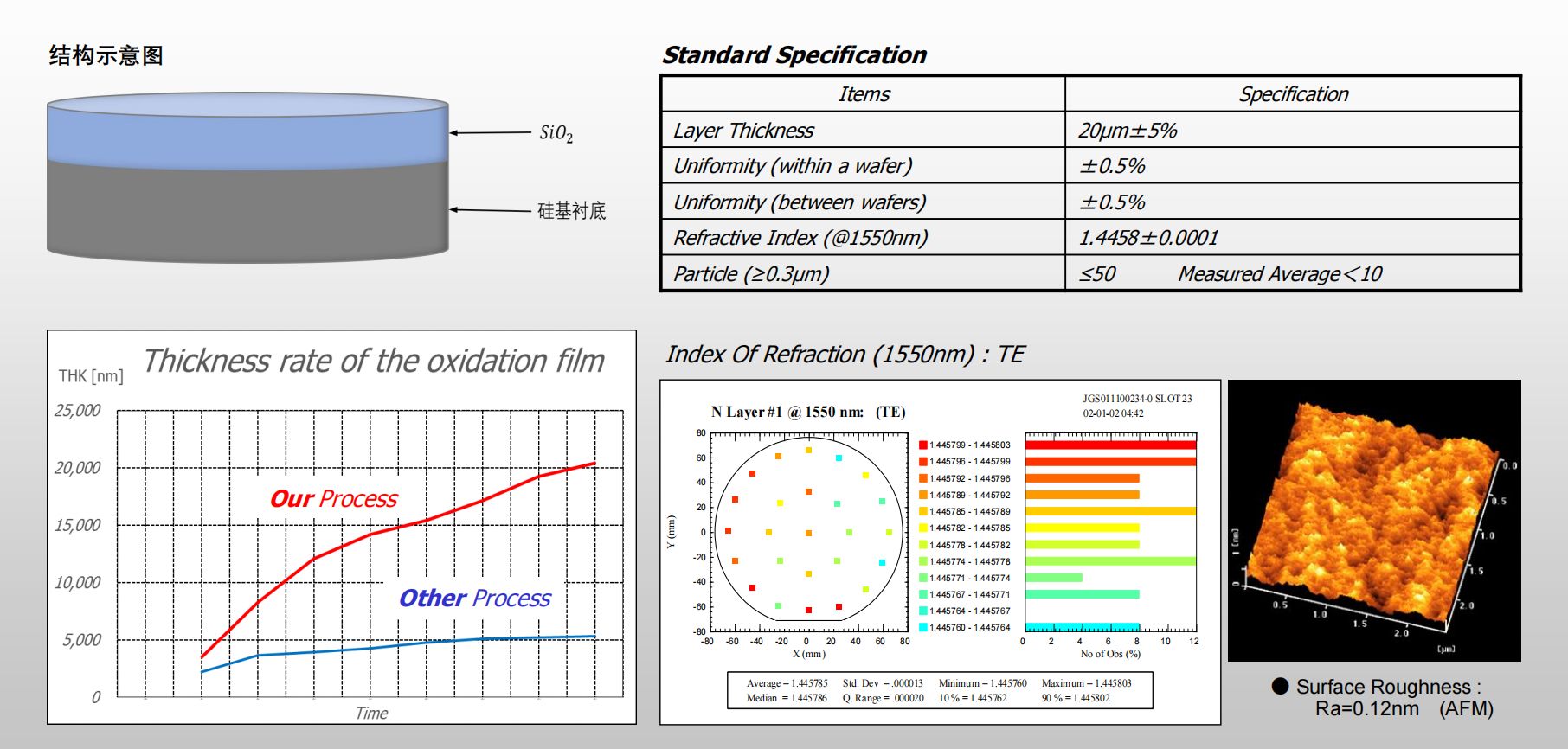
Detailed Diagram