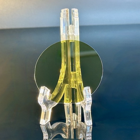
4 inch SiC Wafers 6H Semi-Insulating SiC Substrates prime, research, and dummy grade

Product Specification
| Grade |
Zero MPD Production Grade (Z Grade) |
Standard Production Grade(P Grade) |
Dummy Grade (D Grade) |
||||||||
| Diameter | 99.5 mm~100.0 mm | ||||||||||
| 4H-SI | 500 μm±20 μm |
500 μm±25 μm |
|||||||||
| Wafer Orientation |
Off axis : 4.0° toward< 1120 > ±0.5° for 4H-N, On axis : <0001>±0.5° for 4H-SI |
||||||||||
| 4H-SI |
≤1cm-2 |
≤5 cm-2 |
≤15 cm-2 |
||||||||
| 4H-SI |
≥1E9 Ω·cm |
≥1E5 Ω·cm |
|||||||||
| Primary Flat Orientation |
{10-10} ±5.0° |
||||||||||
| Primary Flat Length | 32.5 mm±2.0 mm | ||||||||||
| Secondary Flat Length | 18.0 mm±2.0 mm | ||||||||||
| Secondary Flat Orientation |
Silicon face up: 90° CW. from Prime flat ±5.0° |
||||||||||
| Edge Exclusion |
3 mm |
||||||||||
| LTV/TTV/Bow /Warp | ≤3 μm/≤5 μm/≤15 μm/≤30 μm | ≤10 μm/≤15 μm/≤25 μm/≤40 μm | |||||||||
|
Roughness |
C face |
Polish | Ra≤1 nm | ||||||||
|
Si face |
CMP | Ra≤0.2 nm |
Ra≤0.5 nm |
||||||||
| Edge Cracks By High Intensity Light |
None |
Cumulative length ≤ 10 mm, single length≤2 mm |
|||||||||
| Hex Plates By High Intensity Light | Cumulative area ≤0.05% | Cumulative area ≤0.1% | |||||||||
| Polytype Areas By High Intensity Light |
None |
Cumulative area≤3% | |||||||||
| Visual Carbon Inclusions | Cumulative area ≤0.05% | Cumulative area ≤3% | |||||||||
| Silicon Surface Scratches By High Intensity Light |
None |
Cumulative length≤1*wafer diameter | |||||||||
| Edge Chips High By Intensity Light | None permitted ≥0.2 mm width and depth | 5 allowed, ≤1 mm each | |||||||||
| Silicon Surface Contamination By High Intensity |
None |
||||||||||
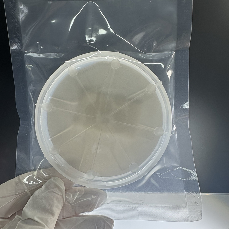
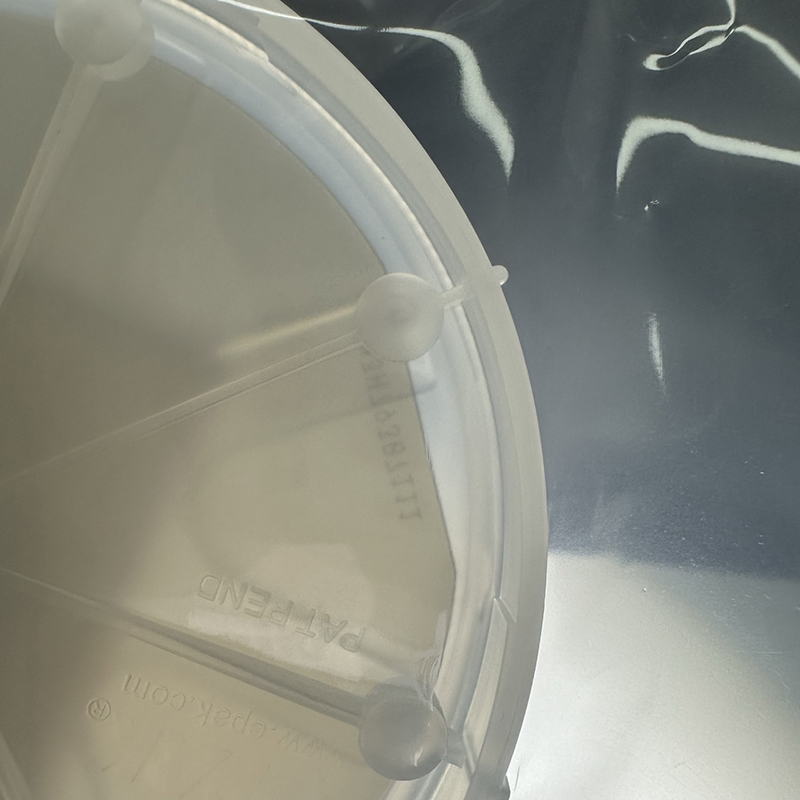
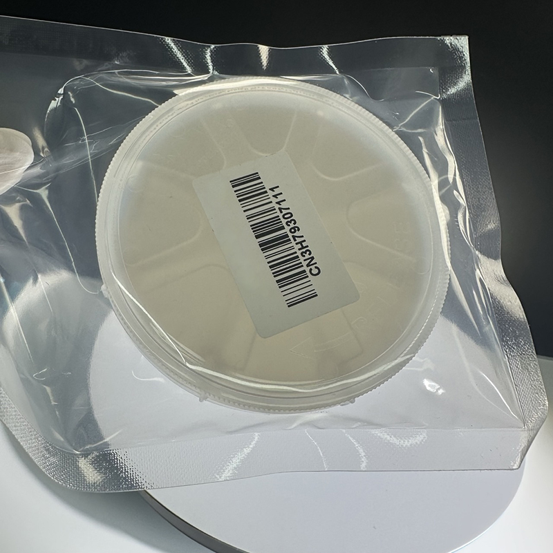
| Packaging |
Multi-wafer Cassette Or Single Wafer Container |
||||||||||
Detailed Diagram
Related Products


Write your message here and send it to us