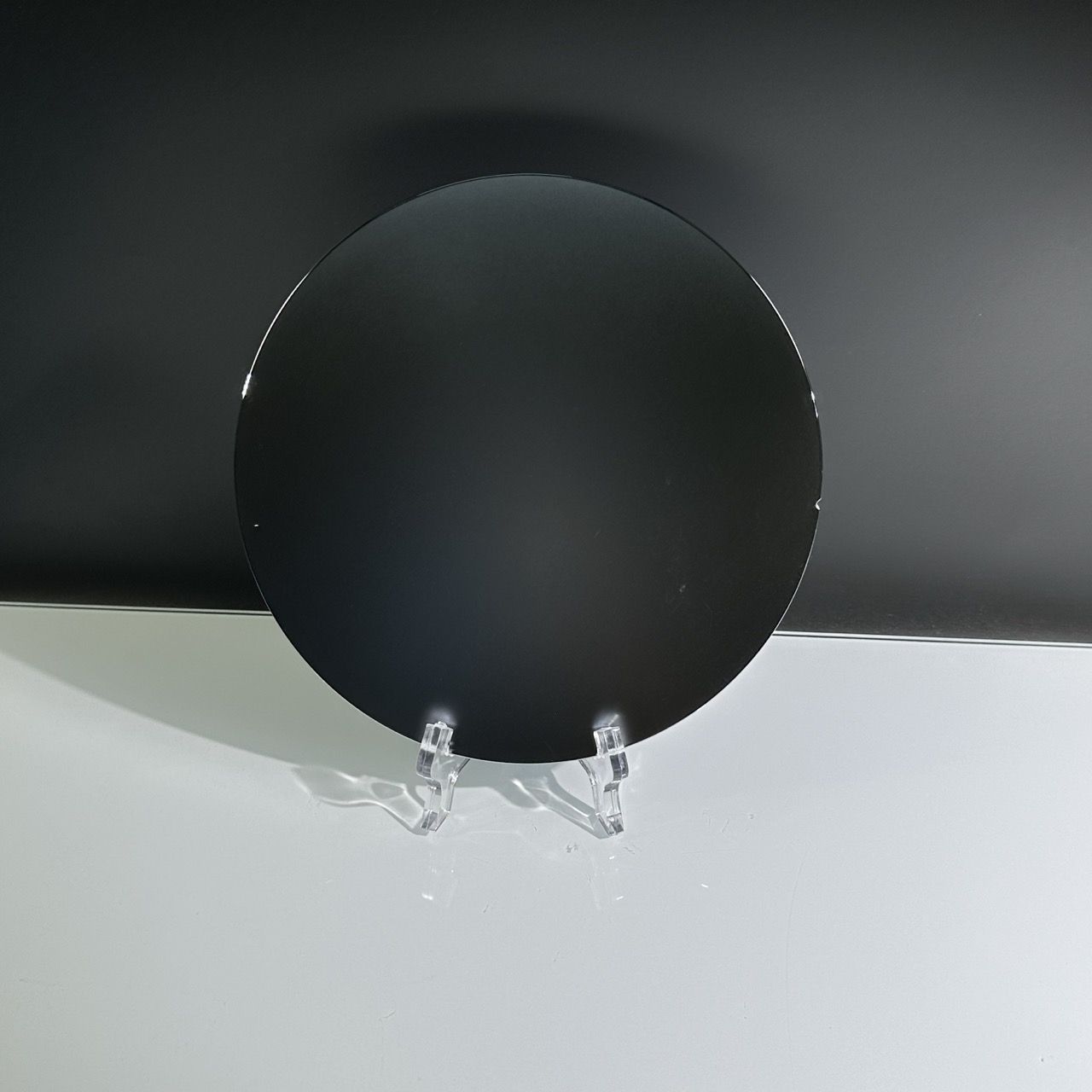
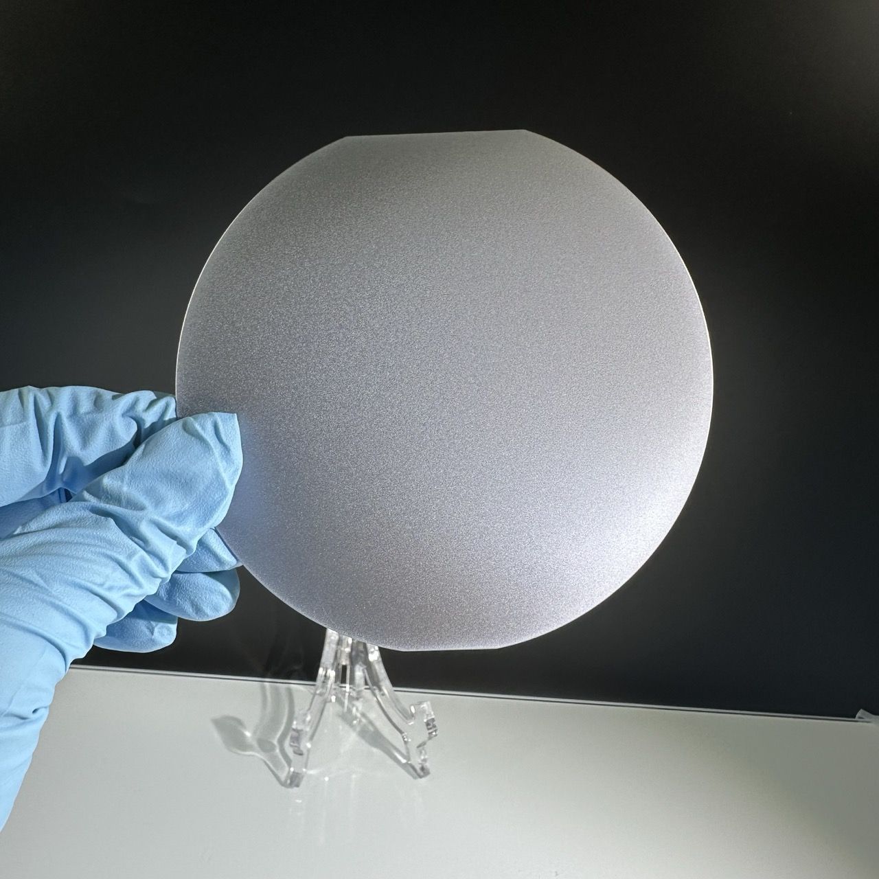
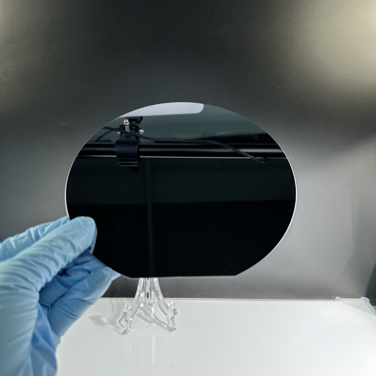
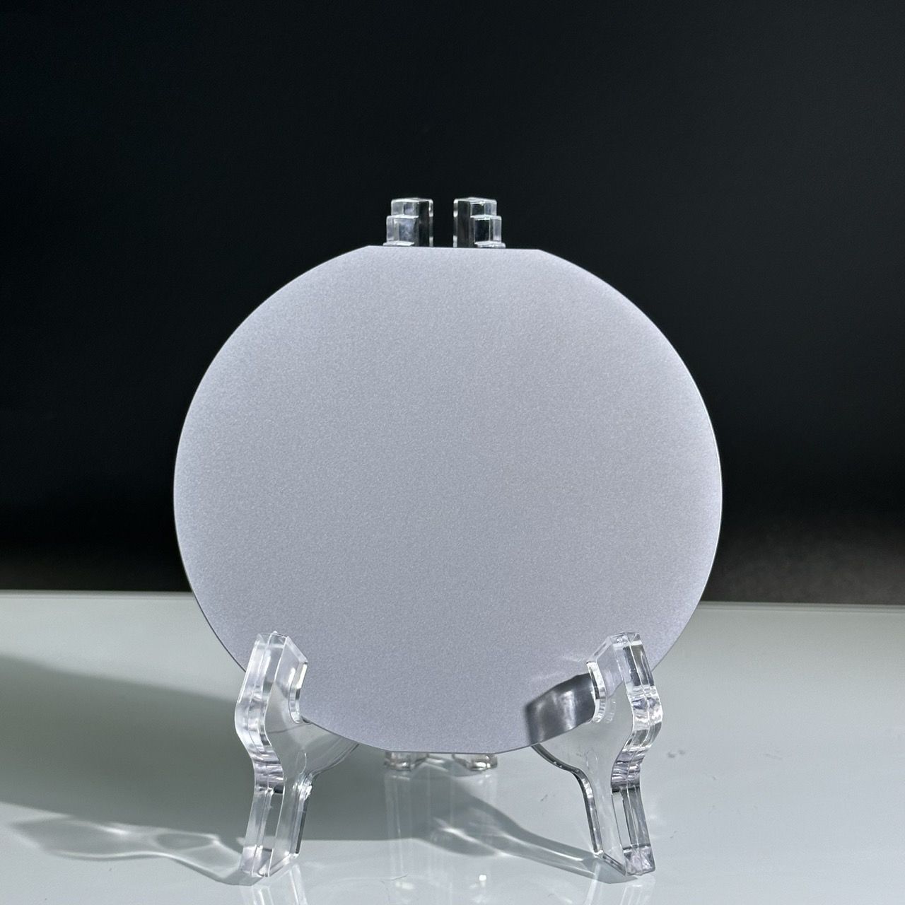
6inch N-Type or P-type Silicon wafer CZ Si wafer


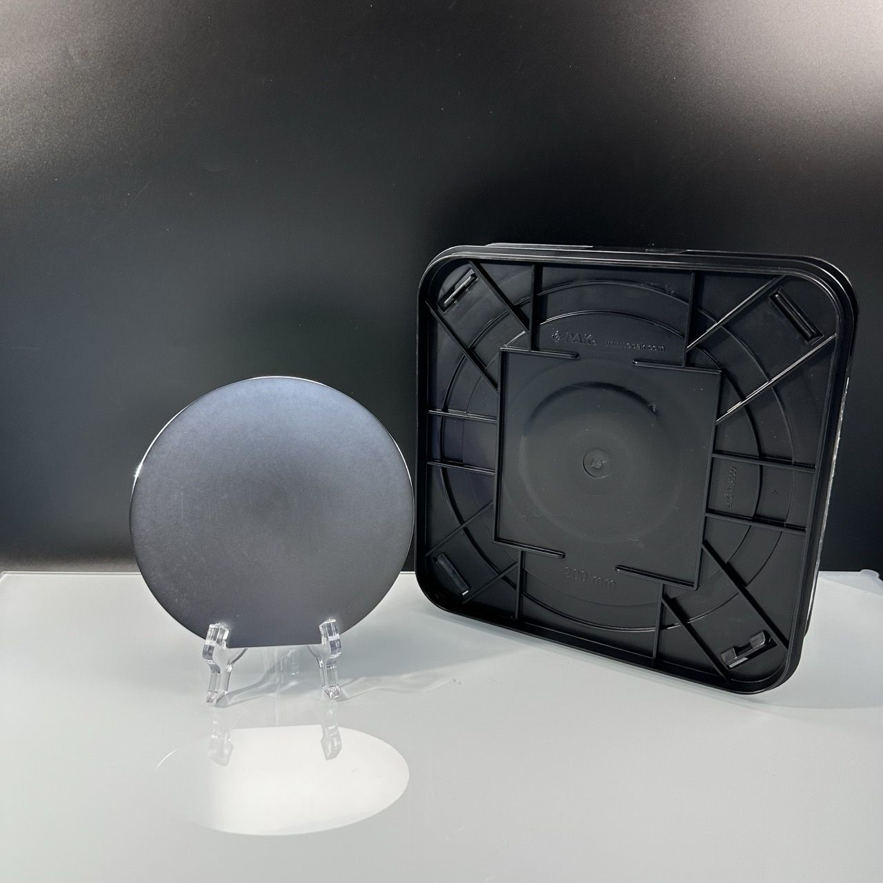
Introduce of wafer box
The Specifications of Silicon wafer:
6inch Silicon wafer Growth: CZ, MCZ, FZ。
6 Silicon wafer Grade: Prime, Test, Dummy, etc
6inch Silicon wafer Diameter: 6 inch/150mm。
6inch Silicon wafer Thickness: 200~ 3000um。
6inch Silicon wafer Finish: As cut, lapped, etched, SSP, DSP, etc。
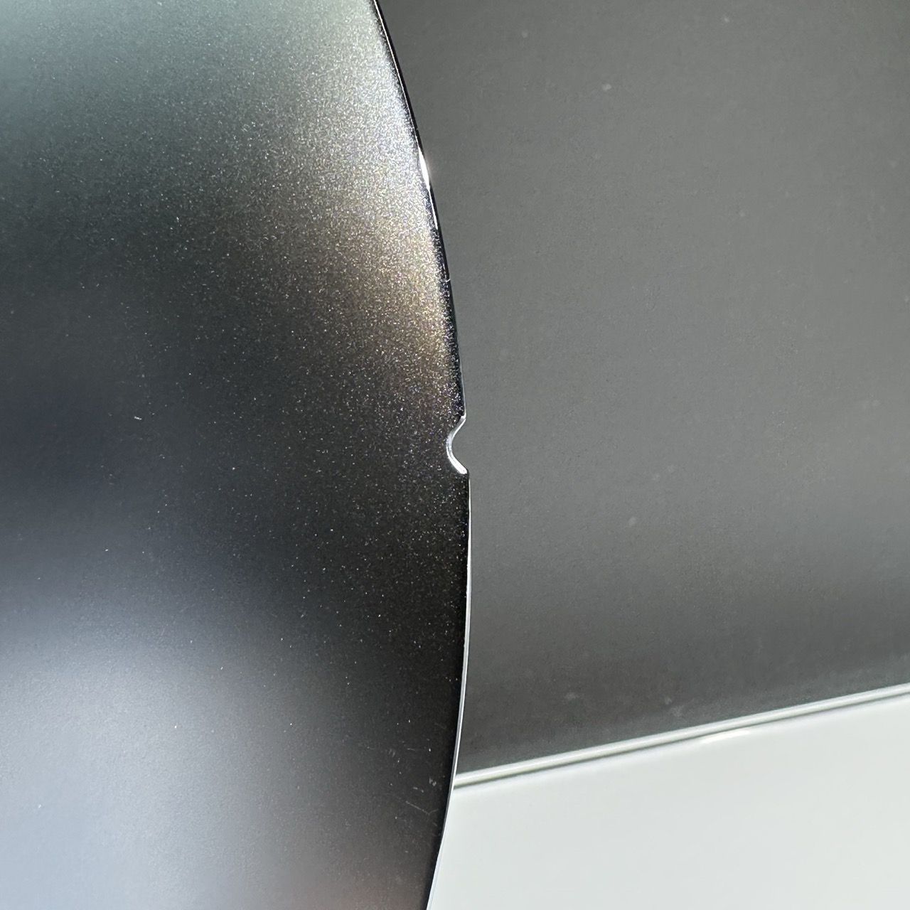
6inch Silicon wafer Orientation: (100) (111) (110) (531)(553) etc。
6inch Silicon wafer Off cut: up to 4deg。
6inch Silicon wafer Type/Dopant: P/B, N/Phos, N/As, N/Sb, Intrinsic。
6inch Silicon wafer Resistivity: CZ/MCZ: From 0.001 to 1000 ohm-cm. FZ: up to 20k ohm-cm.
6inch Silicon wafer Thin films: (a)PVD: Al, Cu, Au, Cr, Si, Ni;, Fe, Mo. etc, Coating thicknesses up to 20.000A/5%.
(b)LPCVD/PECVD: Oxide, Nitride, siC, etc,Coating thicknesses up to 200.000A/3%.
(c)Silicon epitaxial wafers and epitaxial services(SOS, GaN, GOI etc).
6inch Silicon wafer Processes: a.DSP, ultra thin, ultra flat, etc.
b.Downsizing, back grinding, dicing,etc。c. MEMS.
Since 2010, Shanghai XKH Material Tech. Co.,Ltd has been committed to providing customers with comprehensive 4-inch wafer Silicon Wafer solutions, from debugging level wafers Dummy Wafer, test level wafers Test Wafer, to product level wafers Prime Wafer, as well as special wafers, Oxide wafers Oxide, Nitride wafers Si3N4, Aluminum plated wafers, Copper plated silicon wafers, SOI Wafer, MEMS Glass, customized ultra-thick and ultra-flat wafers, etc., with sizes ranging from 50mm-300mm, and we can provide semiconductor wafers with single-sided/double-sided polishing, thinning, dicing, MEMS and other processing and customization services.
Detailed Diagram