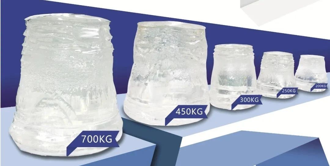
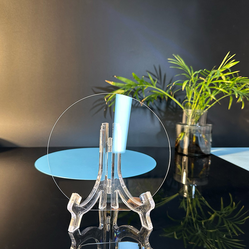
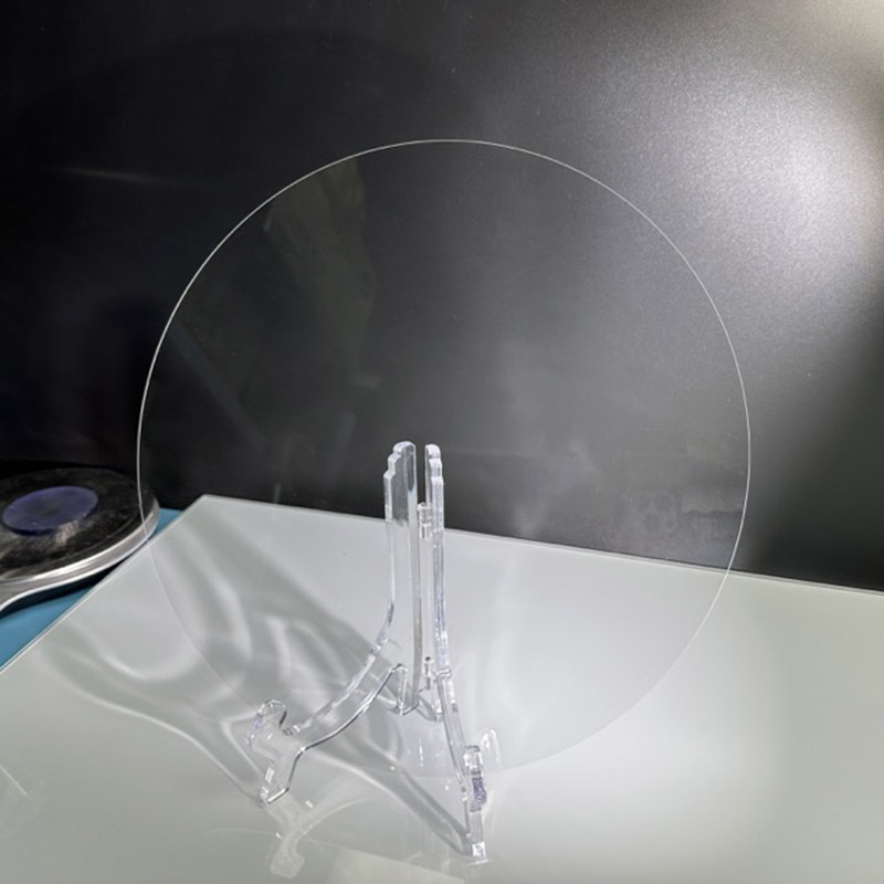
Dia300x1.0mmt Thickness Sapphire Wafer C-Plane SSP/DSP

Introduce of wafer box
| Crystal Materials | 99,999% of Al2O3,High Purity, Monocrystalline, Al2O3 | |||
| Crystal quality | Inclusions, block marks, twins, Color, micro-bubbles and dispersal centers are non-existent | |||
| Diameter | 2inch | 3inch | 4inch | 6inch ~ 12inch |
| 50.8± 0.1mm | 76.2±0.2mm | 100±0.3mm | In accordance with the provisions of standard production | |
| Thickness | 430±15µm | 550±15µm | 650±20µm | Can be customized by customer |
| Orientation | C- plane (0001) to M-plane (1-100) or A-plane(1 1-2 0) 0.2±0.1° /0.3±0.1°, R-plane (1-1 0 2), A-plane (1 1-2 0 ), M-plane(1-1 0 0), Any Orientation , Any angle | |||
| Primary flat length | 16.0±1mm | 22.0±1.0mm | 32.5±1.5 mm | In accordance with the provisions of standard production |
| Primary flat Orientation | A-plane (1 1-2 0 ) ± 0.2° | |||
| TTV | ≤10µm | ≤15µm | ≤20µm | ≤30µm |
| LTV | ≤10µm | ≤15µm | ≤20µm | ≤30µm |
| TIR | ≤10µm | ≤15µm | ≤20µm | ≤30µm |
| BOW | ≤10µm | ≤15µm | ≤20µm | ≤30µm |
| Warp | ≤10µm | ≤15µm | ≤20µm | ≤30µm |
| Front Surface | Epi-Polished (Ra< 0.2nm) | |||
*Bow: The deviation of the center point of the median surface of a free, un-clamped wafer from the reference plane, where the reference plane is defined by the three corners of an equilateral triangle.
*Warp: The difference between the maximum and the minimum distances of the median surface of a free, un-clamped wafer from the reference plane defined above.
High-quality products and services for next-generation semiconductor devices and epitaxial growth:
High degree of flatness (controlled TTV, bow, warp etc.)
High-quality cleaning (low particle contamination, low metal contamination)
Substrate drilling, grooving, cutting, and backside polishing
Attachment of data such as cleanliness and shape of substrate (optional)
If you have a need for sapphire substrates, please feel free to contact:
mail:eric@xkh-semitech.com +86 158 0194 2596 /doris@xkh-semitech.com +86 187 0175 6522
We will back to you asap!
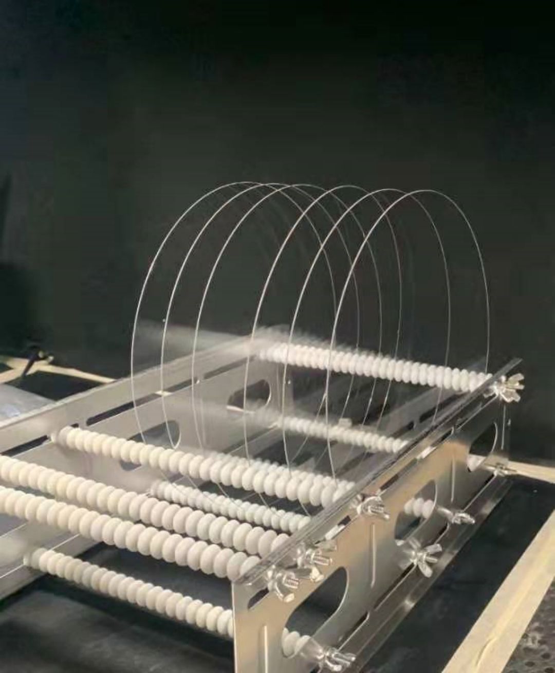
Detailed Diagram