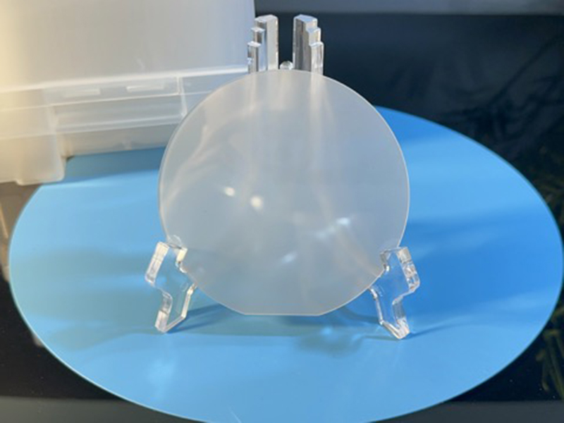
2 inch 50.8mm Sapphire Wafer C-Plane M-plane R-plane A-plane


Description
Sapphire crystal is widely used in semiconductor (MOCVD gallium nitride epitaxy substrate), watches, medical, communications, laser, infrared, electronics, measuring instruments, military and aerospace and many other cutting-edge high-tech fields. Our company produces high precision sapphire wafer with thickness ≧0.1mm and external dimension ≧Φ1" for a long time. In addition to the conventional Φ2 ", Φ3 ", Φ4 ", Φ6 ", Φ8 ", Φ12 ", other sizes can be customized, please contact our sales staff.
Dimension: 2inch, 3inch, 4inch, 6inch, 8inch, 12inch
Thickness: 100um, 280um, 300um, 350um, 430um, 500um, 650um, 1mm or others
Orientation: C-Axis, M-Axis, R-Axis, A-Axis C miscut A or others
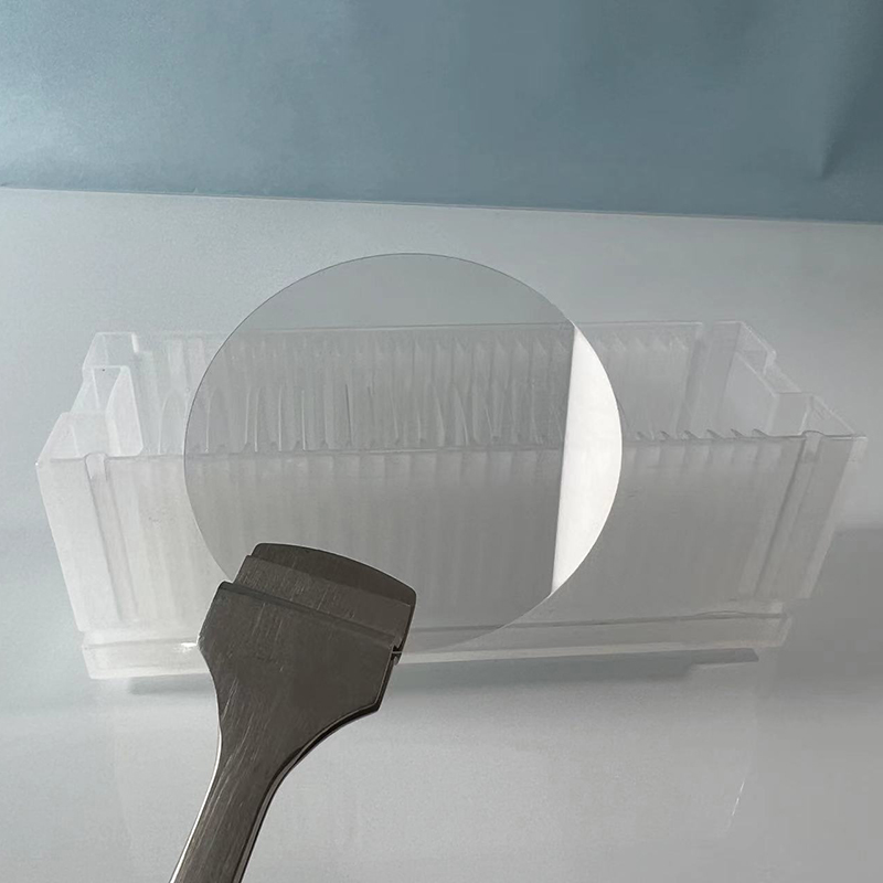
Surface: SSP, DSP, Grinding
Description: Sapphire is a single crystal of alumina, which is the second hardest material in nature, second only to diamond. Sapphire has good light transmission, high strength, collision resistance, wear resistance, corrosion resistance and resistance to high temperature and pressure, biocompatibility, can be made into various shapes of objects. It is an ideal substrate material for making semiconductor optoelectronic devices.
Application
Sapphire single crystal is an excellent multi-functional material. It can be widely used in many fields such as industry, defense and scientific research (such as high temperature resistant infrared window). At the same time, it is also a widely used single crystal substrate material. It is the preferred substrate for the current blue, purple, white light emitting diode (LED) and blue laser (LD) industry (need to epitaxy gallium nitride film layer on the sapphire substrate), and is also an important superconducting thin film substrate. In addition to the production of Y- series, La- series and other high-temperature superconducting films, it can also be used to grow new practical MgB2 (magnesium diboride) superconducting films.
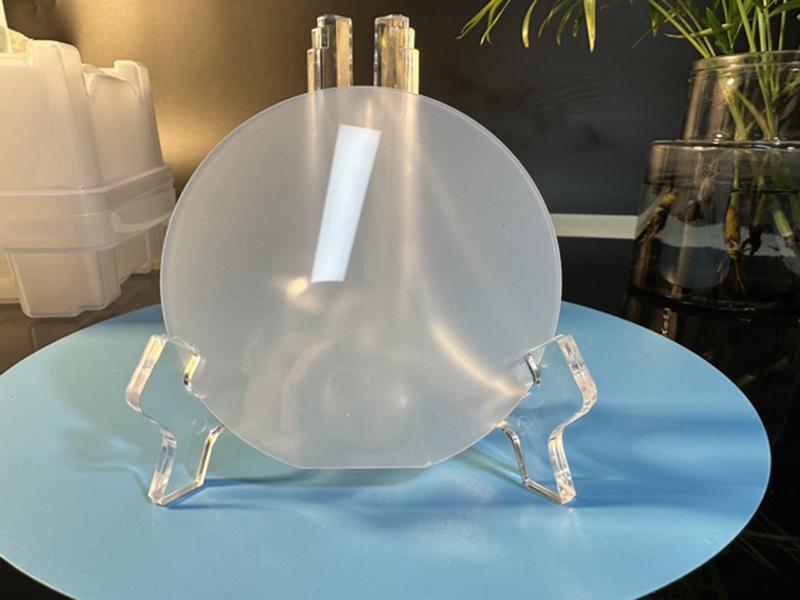
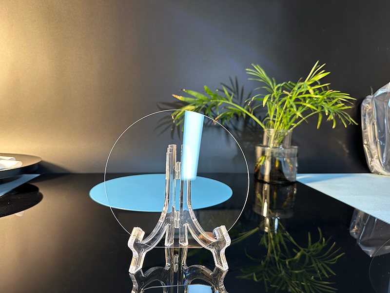
Detailed Diagram