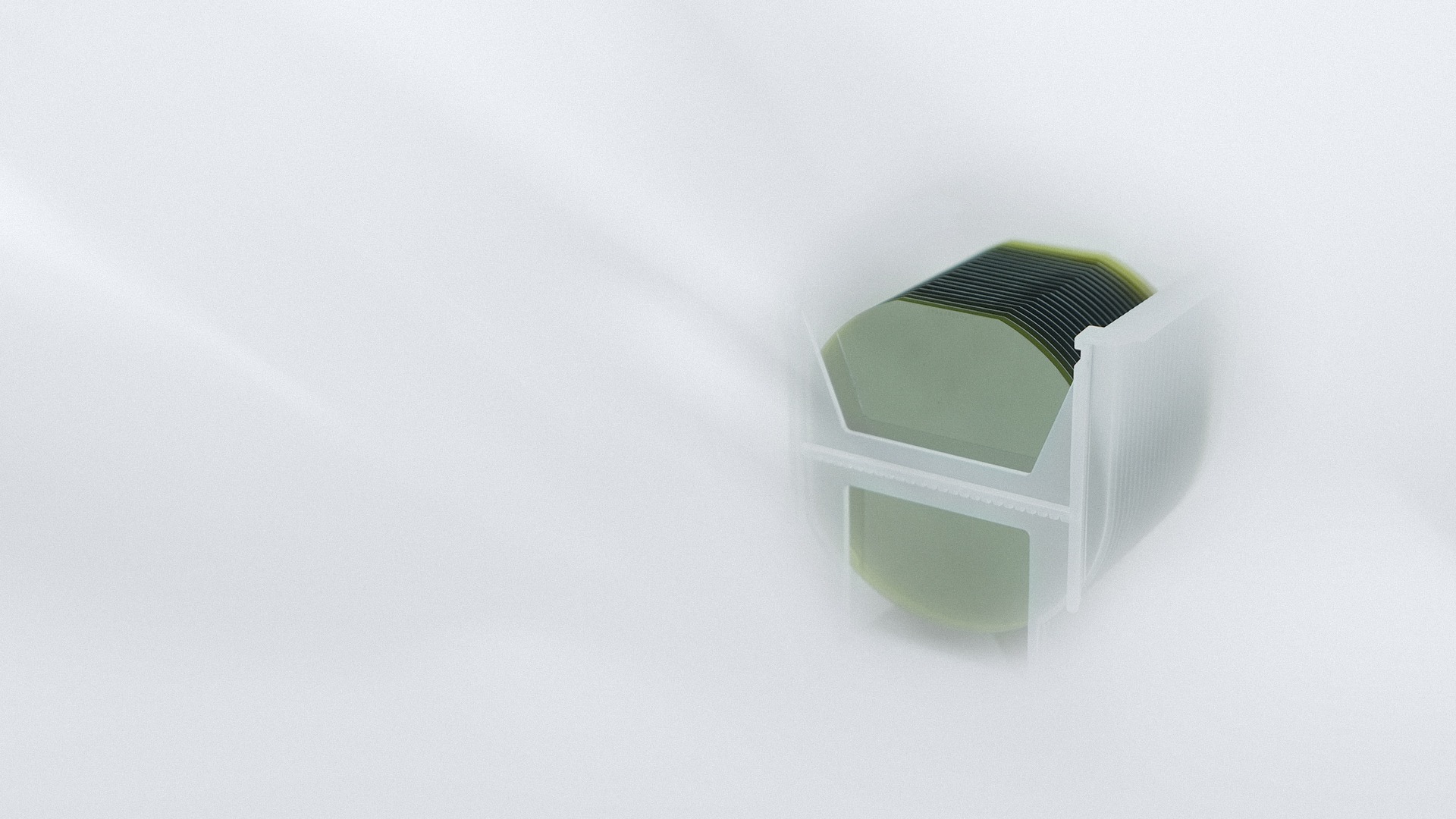
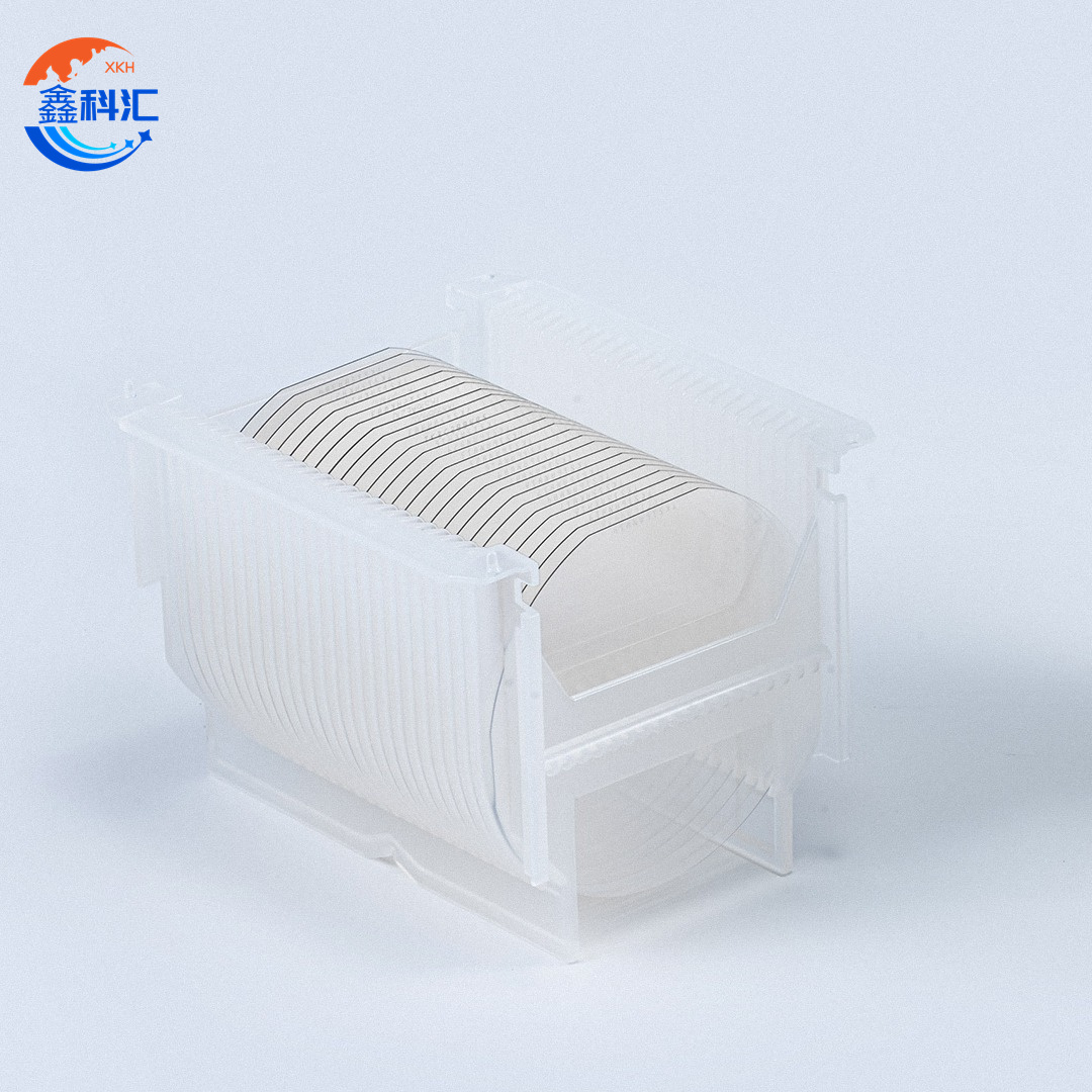
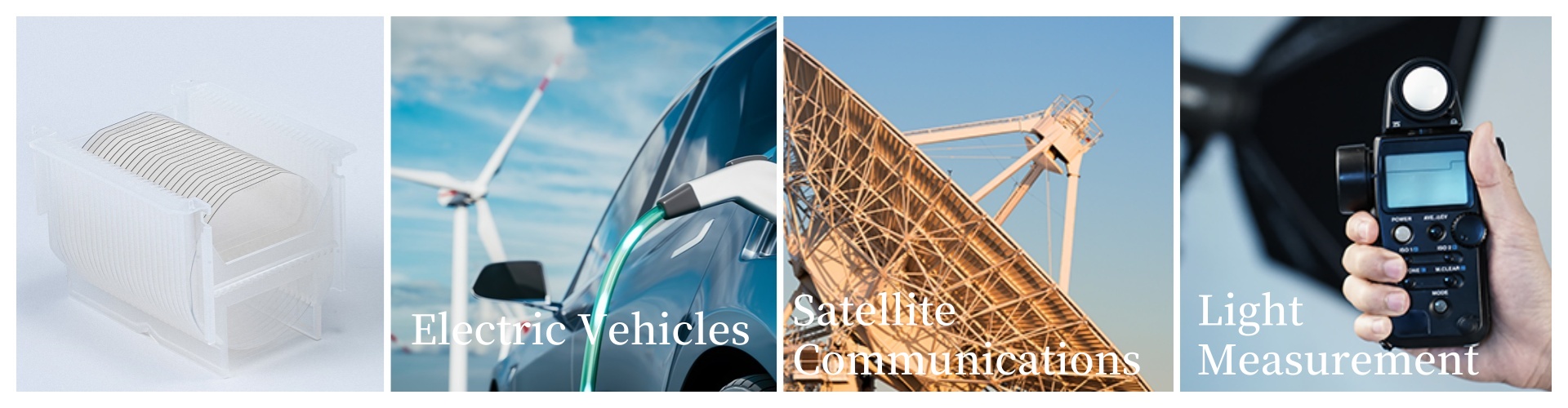
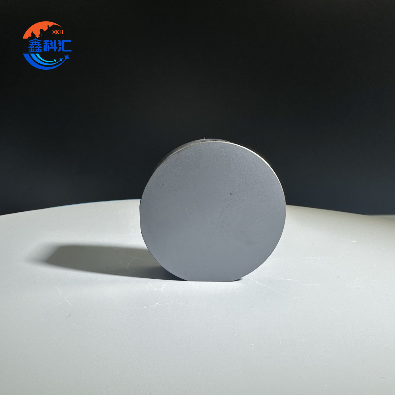
4H-N HPSI SiC wafer 6H-N 6H-P 3C-N SiC Epitaxial wafer for MOS or SBD


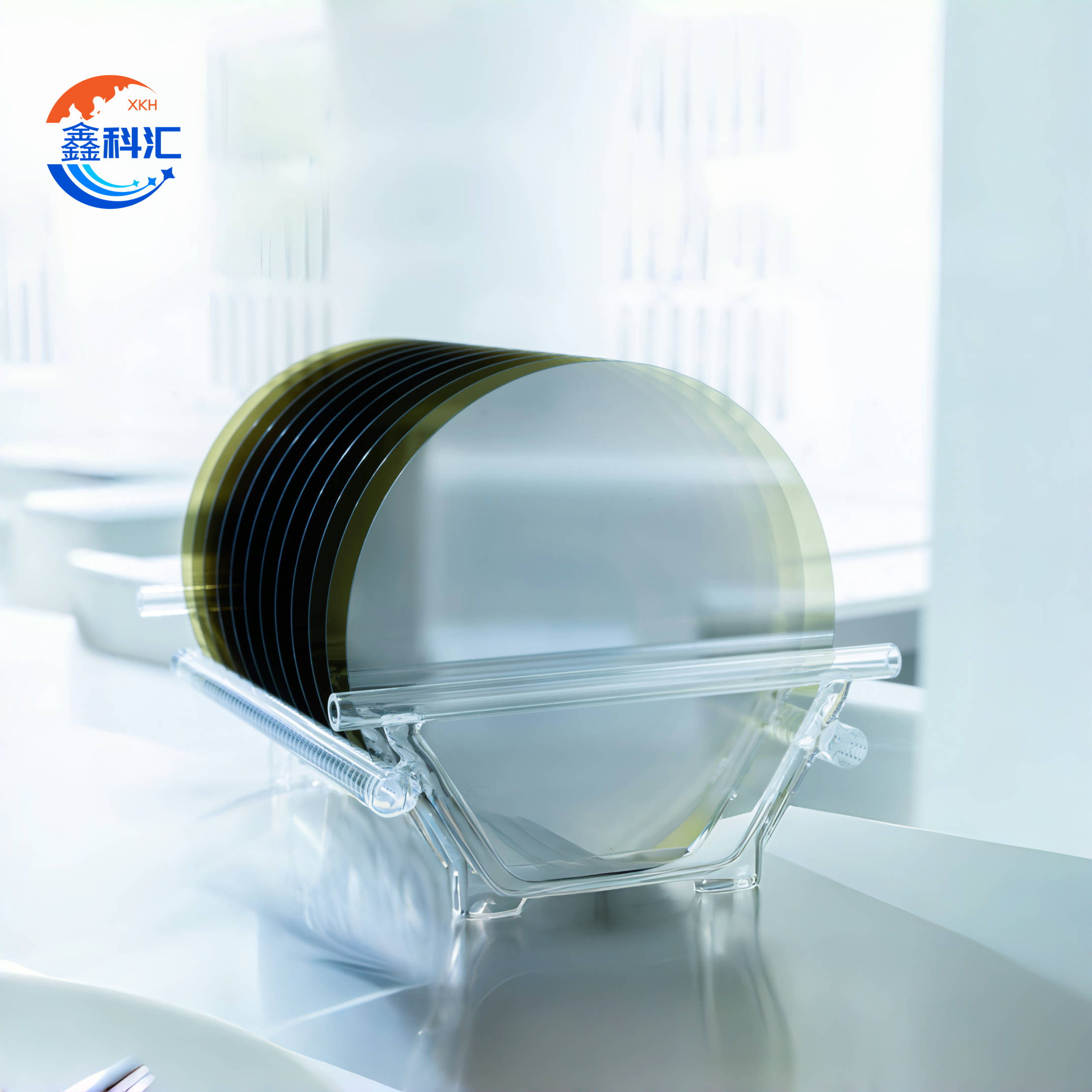
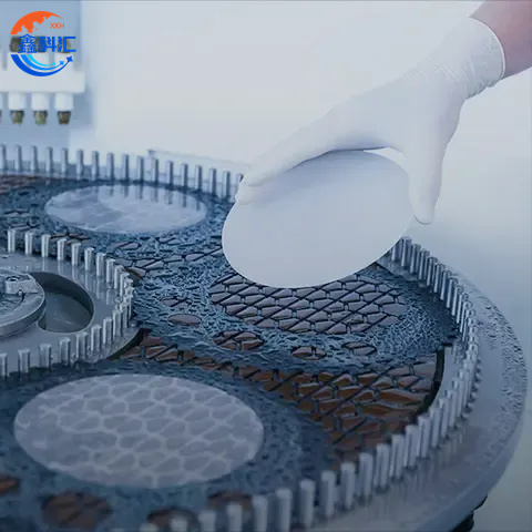
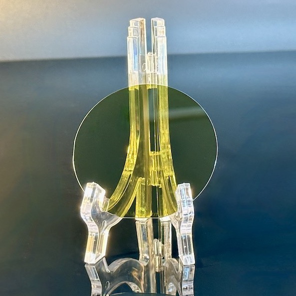
SiC Substrate SiC Epi-wafer Brief
We offer a full portfolio of high-quality SiC substrates and sic wafers in multiple polytypes and doping profiles—including 4H-N (n-type conductive), 4H-P (p-type conductive), 4H-HPSI (high-purity semi-insulating), and 6H-P (p-type conductive)—in diameters from 4″, 6″, and 8″ all the way up to 12″. Beyond bare substrates, our value-added epi wafer growth services deliver epitaxial (epi) wafers with tightly controlled thickness (1–20 µm), doping concentrations, and defect densities.
Each sic wafer and epi wafer undergoes rigorous in-line inspection (micropipe density <0.1 cm⁻², surface roughness Ra <0.2 nm) and full electrical characterization (CV, resistivity mapping) to ensure exceptional crystal uniformity and performance. Whether used for power electronics modules, high-frequency RF amplifiers, or optoelectronic devices (LEDs, photodetectors), our SiC substrate and epi wafer product lines deliver the reliability, thermal stability, and breakdown strength required by today’s most demanding applications.
SiC Substrate 4H-N type‘s properties and application
-
4H-N SiC substrate Polytype (Hexagonal) Structure
Wide bandgap of ~3.26 eV ensures stable electrical performance and thermal robustness under high-temperature and high-electric-field conditions.
-
SiC substrate N-Type Doping
Precisely controlled nitrogen doping yields carrier concentrations from 1×10¹⁶ to 1×10¹⁹ cm⁻³ and room-temperature electron mobilities up to ~900 cm²/V·s, minimizing conduction losses.
-
SiC substrate Wide Resistivity & Uniformity
Available resistivity range of 0.01–10 Ω·cm and wafer thicknesses of 350–650 µm with ±5% tolerance in both doping and thickness—ideal for high-power device fabrication.
-
SiC substrate Ultra-Low Defect Density
Micropipe density < 0.1 cm⁻² and basal-plane dislocation density < 500 cm⁻², delivering > 99% device yield and superior crystal integrity.
- SiC substrate Exceptional Thermal Conductivity
Thermal conductivity up to ~370 W/m·K facilitates efficient heat removal, boosting device reliability and power density.
-
SiC substrateTarget Applications
SiC MOSFETs, Schottky diodes, power modules and RF devices for electric-vehicle drives, solar inverters, industrial drives, traction systems, and other demanding power-electronics markets.
6inch 4H-N type SiC wafer's specification |
||
| Property | Zero MPD Production Grade (Z Grade) | Dummy Grade (D Grade) |
| Grade | Zero MPD Production Grade (Z Grade) | Dummy Grade (D Grade) |
| Diameter | 149.5 mm - 150.0 mm | 149.5 mm - 150.0 mm |
| Poly-type | 4H | 4H |
| Thickness | 350 µm ± 15 µm | 350 µm ± 25 µm |
| Wafer Orientation | Off axis: 4.0° toward <1120> ± 0.5° | Off axis: 4.0° toward <1120> ± 0.5° |
| Micropipe Density | ≤ 0.2 cm² | ≤ 15 cm² |
| Resistivity | 0.015 - 0.024 Ω·cm | 0.015 - 0.028 Ω·cm |
| Primary Flat Orientation | [10-10] ± 50° | [10-10] ± 50° |
| Primary Flat Length | 475 mm ± 2.0 mm | 475 mm ± 2.0 mm |
| Edge Exclusion | 3 mm | 3 mm |
| LTV/TIV / Bow / Warp | ≤ 2.5 µm / ≤ 6 µm / ≤ 25 µm / ≤ 35 µm | ≤ 5 µm / ≤ 15 µm / ≤ 40 µm / ≤ 60 µm |
| Roughness | Polish Ra ≤ 1 nm | Polish Ra ≤ 1 nm |
| CMP Ra | ≤ 0.2 nm | ≤ 0.5 nm |
| Edge Cracks By High Intensity Light | Cumulative length ≤ 20 mm single length ≤ 2 mm | Cumulative length ≤ 20 mm single length ≤ 2 mm |
| Hex Plates By High Intensity Light | Cumulative area ≤ 0.05% | Cumulative area ≤ 0.1% |
| Polytype Areas By High Intensity Light | Cumulative area ≤ 0.05% | Cumulative area ≤ 3% |
| Visual Carbon Inclusions | Cumulative area ≤ 0.05% | Cumulative area ≤ 5% |
| Silicon Surface Scratches By High Intensity Light | Cumulative length ≤ 1 wafer diameter | |
| Edge Chips By High Intensity Light | None permitted ≥ 0.2 mm width and depth | 7 allowed, ≤ 1 mm each |
| Threading Screw Dislocation | < 500 cm³ | < 500 cm³ |
| Silicon Surface Contamination By High Intensity Light | ||
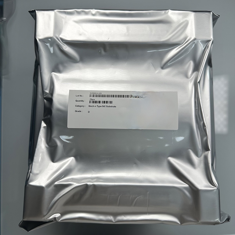
| Packaging | Multi-wafer Cassette Or Single Wafer Container | Multi-wafer Cassette Or Single Wafer Container |
8inch 4H-N type SiC wafer's specification |
||
| Property | Zero MPD Production Grade (Z Grade) | Dummy Grade (D Grade) |
| Grade | Zero MPD Production Grade (Z Grade) | Dummy Grade (D Grade) |
| Diameter | 199.5 mm - 200.0 mm | 199.5 mm - 200.0 mm |
| Poly-type | 4H | 4H |
| Thickness | 500 µm ± 25 µm | 500 µm ± 25 µm |
| Wafer Orientation | 4.0° toward <110> ± 0.5° | 4.0° toward <110> ± 0.5° |
| Micropipe Density | ≤ 0.2 cm² | ≤ 5 cm² |
| Resistivity | 0.015 - 0.025 Ω·cm | 0.015 - 0.028 Ω·cm |
| Noble Orientation | ||
| Edge Exclusion | 3 mm | 3 mm |
| LTV/TIV / Bow / Warp | ≤ 5 µm / ≤ 15 µm / ≤ 35 µm / 70 µm | ≤ 5 µm / ≤ 15 µm / ≤ 35 µm / 100 µm |
| Roughness | Polish Ra ≤ 1 nm | Polish Ra ≤ 1 nm |
| CMP Ra | ≤ 0.2 nm | ≤ 0.5 nm |
| Edge Cracks By High Intensity Light | Cumulative length ≤ 20 mm single length ≤ 2 mm | Cumulative length ≤ 20 mm single length ≤ 2 mm |
| Hex Plates By High Intensity Light | Cumulative area ≤ 0.05% | Cumulative area ≤ 0.1% |
| Polytype Areas By High Intensity Light | Cumulative area ≤ 0.05% | Cumulative area ≤ 3% |
| Visual Carbon Inclusions | Cumulative area ≤ 0.05% | Cumulative area ≤ 5% |
| Silicon Surface Scratches By High Intensity Light | Cumulative length ≤ 1 wafer diameter | |
| Edge Chips By High Intensity Light | None permitted ≥ 0.2 mm width and depth | 7 allowed, ≤ 1 mm each |
| Threading Screw Dislocation | < 500 cm³ | < 500 cm³ |
| Silicon Surface Contamination By High Intensity Light | ||
| Packaging | Multi-wafer Cassette Or Single Wafer Container | Multi-wafer Cassette Or Single Wafer Container |
4H-SiC is a high-performance material used for power electronics, RF devices, and high-temperature applications. The "4H" refers to the crystal structure, which is hexagonal, and the "N" indicates a doping type used to optimize the material’s performance.
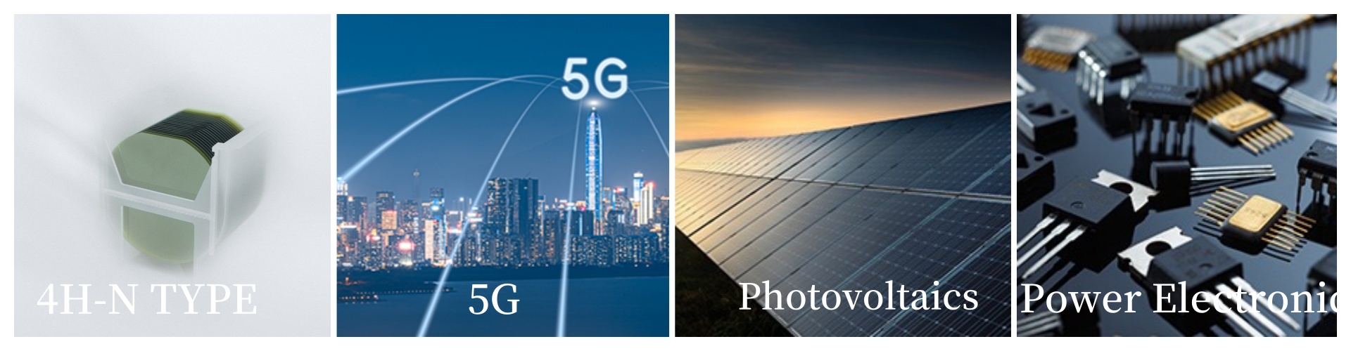
The 4H-SiC type is commonly utilized for:
Power Electronics: Used in devices like diodes, MOSFETs, and IGBTs for electric vehicle powertrains, industrial machinery, and renewable energy systems.
5G Technology: With 5G's demand for high-frequency and high-efficiency components, SiC's ability to handle high voltages and operate at high temperatures makes it ideal for base station power amplifiers and RF devices.
Solar Energy Systems: SiC’s excellent power handling properties are ideal for photovoltaic (solar power) inverters and converters.
Electric Vehicles (EVs): SiC is widely used in EV powertrains for more efficient energy conversion, lower heat generation, and higher power densities.
SiC Substrate 4H Semi-Insulating type‘s properties and application
Properties:
-
Micropipe-free density control techniques: Ensures the absence of micropipes, improving the substrate quality.
-
Monocrystalline control techniques: Guarantees a single crystal structure for enhanced material properties.
-
Inclusions control techniques: Minimizes the presence of impurities or inclusions, ensuring a pure substrate.
-
Resistivity control techniques: Allows for precise control of electrical resistivity, which is crucial for device performance.
-
Impurity regulation and control techniques: Regulates and limits the introduction of impurities to maintain substrate integrity.
-
Substrate step width control techniques: Provides accurate control over step width, ensuring consistency across the substrate
6Inch 4H-semi SiC substrate specification |
||
| Property | Zero MPD Production Grade (Z Grade) | Dummy Grade (D Grade) |
| Diameter (mm) | 145 mm - 150 mm | 145 mm - 150 mm |
| Poly-type | 4H | 4H |
| Thickness (um) | 500 ± 15 | 500 ± 25 |
| Wafer Orientation | On axis: ±0.0001° | On axis: ±0.05° |
| Micropipe Density | ≤ 15 cm-2 | ≤ 15 cm-2 |
| Resistivity (Ωcm) | ≥ 10E3 | ≥ 10E3 |
| Primary Flat Orientation | (0-10)° ± 5.0° | (10-10)° ± 5.0° |
| Primary Flat Length | Notch | Notch |
| Edge Exclusion (mm) | ≤ 2.5 µm / ≤ 15 µm | ≤ 5.5 µm / ≤ 35 µm |
| LTV / Bowl / Warp | ≤ 3 µm | ≤ 3 µm |
| Roughness | Polish Ra ≤ 1.5 µm | Polish Ra ≤ 1.5 µm |
| Edge Chips By High Intensity Light | ≤ 20 µm | ≤ 60 µm |
| Heat Plates By High Intensity Light | Cumulative ≤ 0.05% | Cumulative ≤ 3% |
| Polytype Areas By High Intensity Light | Visual Carbon Inclusions ≤ 0.05% | Cumulative ≤ 3% |
| Silicon Surface Scratches By High Intensity Light | ≤ 0.05% | Cumulative ≤ 4% |
| Edge Chips By High Intensity Light (Size) | Not Permitted > 02 mm Width and Depth | Not Permitted > 02 mm Width and Depth |
| The Aiding Screw Dilation | ≤ 500 µm | ≤ 500 µm |
| Silicon Surface Contamination By High Intensity Light | ≤ 1 x 10^5 | ≤ 1 x 10^5 |
| Packaging | Multi-wafer Cassette or Single Wafer Container | Multi-wafer Cassette or Single Wafer Container |
4-Inch 4H-Semi Insulating SiC Substrate Specification
| Parameter | Zero MPD Production Grade (Z Grade) | Dummy Grade (D Grade) |
|---|---|---|
| Physical Properties | ||
| Diameter | 99.5 mm – 100.0 mm | 99.5 mm – 100.0 mm |
| Poly-type | 4H | 4H |
| Thickness | 500 μm ± 15 μm | 500 μm ± 25 μm |
| Wafer Orientation | On axis: <600h > 0.5° | On axis: <000h > 0.5° |
| Electrical Properties | ||
| Micropipe Density (MPD) | ≤1 cm⁻² | ≤15 cm⁻² |
| Resistivity | ≥150 Ω·cm | ≥1.5 Ω·cm |
| Geometric Tolerances | ||
| Primary Flat Orientation | (0x10) ± 5.0° | (0x10) ± 5.0° |
| Primary Flat Length | 52.5 mm ± 2.0 mm | 52.5 mm ± 2.0 mm |
| Secondary Flat Length | 18.0 mm ± 2.0 mm | 18.0 mm ± 2.0 mm |
| Secondary Flat Orientation | 90° CW from Prime flat ± 5.0° (Si face up) | 90° CW from Prime flat ± 5.0° (Si face up) |
| Edge Exclusion | 3 mm | 3 mm |
| LTV / TTV / Bow / Warp | ≤2.5 μm / ≤5 μm / ≤15 μm / ≤30 μm | ≤10 μm / ≤15 μm / ≤25 μm / ≤40 μm |
| Surface Quality | ||
| Surface Roughness (Polish Ra) | ≤1 nm | ≤1 nm |
| Surface Roughness (CMP Ra) | ≤0.2 nm | ≤0.2 nm |
| Edge Cracks (High-Intensity Light) | Not permitted | Cumulative length ≥10 mm, single crack ≤2 mm |
| Hexagonal Plate Defects | ≤0.05% cumulative area | ≤0.1% cumulative area |
| Polytype Inclusion Areas | Not permitted | ≤1% cumulative area |
| Visual Carbon Inclusions | ≤0.05% cumulative area | ≤1% cumulative area |
| Silicon Surface Scratches | Not permitted | ≤1 wafer diameter cumulative length |
| Edge Chips | None allowed (≥0.2 mm width/depth) | ≤5 chips (each ≤1 mm) |
| Silicon Surface Contamination | Not specified | Not specified |
| Packaging | ||
| Packaging | Multi-wafer cassette or single-wafer container | Multi-wafer cassette or |
Application:
The SiC 4H Semi-Insulating substrates are primarily used in high-power and high-frequency electronic devices, especially in the RF field. These substrates are crucial for various applications including microwave communication systems, phased array radar, and wireless electrical detectors. Their high thermal conductivity and excellent electrical characteristics make them ideal for demanding applications in power electronics and communication systems.
SiC epi wafer 4H-N type‘s properties and application
SiC 4H-N Type Epi Wafer Properties and Applications
Properties of SiC 4H-N Type Epi Wafer:
Material Composition:
SiC (Silicon Carbide): Known for its outstanding hardness, high thermal conductivity, and excellent electrical properties, SiC is ideal for high-performance electronic devices.
4H-SiC Polytype: The 4H-SiC polytype is known for its high efficiency and stability in electronic applications.
N-type Doping: N-type doping (doped with nitrogen) provides excellent electron mobility, making SiC suitable for high-frequency and high-power applications.
High Thermal Conductivity:
SiC wafers have superior thermal conductivity, typically ranging from 120–200 W/m·K, allowing them to effectively manage heat in high-power devices like transistors and diodes.
Wide Bandgap:
With a bandgap of 3.26 eV, 4H-SiC can operate at higher voltages, frequencies, and temperatures compared to traditional silicon-based devices, making it ideal for high-efficiency, high-performance applications.
Electrical Properties:
SiC's high electron mobility and conductivity make it ideal for power electronics, offering fast switching speeds and high current and voltage handling capacity, resulting in more efficient power management systems.
Mechanical and Chemical Resistance:
SiC is one of the hardest materials, second only to diamond, and is highly resistant to oxidation and corrosion, making it durable in harsh environments.
Applications of SiC 4H-N Type Epi Wafer:
Power Electronics:
SiC 4H-N type epi wafers are widely used in power MOSFETs, IGBTs, and diodes for power conversion in systems such as solar inverters, electric vehicles, and energy storage systems, offering enhanced performance and energy efficiency.
Electric Vehicles (EVs):
In electric vehicle powertrains, motor controllers, and charging stations, SiC wafers help achieve better battery efficiency, faster charging, and improved overall energy performance due to their ability to handle high power and temperatures.
Renewable Energy Systems:
Solar Inverters: SiC wafers are used in solar energy systems for converting DC power from solar panels to AC, increasing overall system efficiency and performance.
Wind Turbines: SiC technology is employed in wind turbine control systems, optimizing power generation and conversion efficiency.
Aerospace and Defense:
SiC wafers are ideal for use in aerospace electronics and military applications, including radar systems and satellite electronics, where high radiation resistance and thermal stability are crucial.
High-Temperature and High-Frequency Applications:
SiC wafers excel in high-temperature electronics, used in aircraft engines, spacecraft, and industrial heating systems, as they maintain performance in extreme heat conditions. Additionally, their wide bandgap allows for use in high-frequency applications like RF devices and microwave communications.
| 6-inch N-type epit axial specification | |||
| Parameter | unit | Z-MOS | |
| Type | Condutivity / Dopant | - | N-type / Nitrogen |
| Buffer Layer | Buffer Layer Thickness | um | 1 |
| Buffer Layer Thickness Tolerance | % | ±20% | |
| Buffer Layer Concentration | cm-3 | 1.00E+18 | |
| Buffer Layer Concentration Tolerance | % | ±20% | |
| 1st Epi Layer | Epi Layer Thickness | um | 11.5 |
| Epi Layer Thickness Uniformity | % | ±4% | |
| Epi Layers Thickness Tolerance((Spec- Max ,Min)/Spec) |
% | ±5% | |
| Epi Layer Concentration | cm-3 | 1E 15~ 1E 18 | |
| Epi Layer Concentration Tolerance | % | 6% | |
| Epi Layer Concentration Uniformity (σ /mean) |
% | ≤5% | |
| Epi Layer Concentration Uniformity <(max-min)/(max+min> |
% | ≤ 10% | |
| Epitaixal Wafer Shape | Bow | um | ≤±20 |
| WARP | um | ≤30 | |
| TTV | um | ≤ 10 | |
| LTV | um | ≤2 | |
| General Characteristics | Scratches length | mm | ≤30mm |
| Edge Chips | - | NONE | |
| Defects defination | ≥97% (Measured with 2*2, Killer defects inludes: Defects include Micropipe /Large pits, Carrot, Triangular |
||
| Metal contamination | atoms/cm² | d f f ll i ≤5E10 atoms/cm2 (Al, Cr, Fe, Ni, Cu, Zn, Hg,Na,K, Ti, Ca &Mn) |
|
| Package | Packing specifications | pcs/box | multi-wafer cassette or single wafer container |
| 8-inch N-type epitaxial specification | |||
| Parameter | unit | Z-MOS | |
| Type | Condutivity / Dopant | - | N-type / Nitrogen |
| Buffer layer | Buffer Layer Thickness | um | 1 |
| Buffer Layer Thickness Tolerance | % | ±20% | |
| Buffer Layer Concentration | cm-3 | 1.00E+18 | |
| Buffer Layer Concentration Tolerance | % | ±20% | |
| 1st Epi Layer | Epi Layers Thickness Average | um | 8~ 12 |
| Epi Layers Thickness Uniformity (σ/mean) | % | ≤2.0 | |
| Epi Layers Thickness Tolerance((Spec -Max,Min)/Spec) | % | ±6 | |
| Epi Layers Net Average Doping | cm-3 | 8E+15 ~2E+16 | |
| Epi Layers Net Doping Uniformity (σ/mean) | % | ≤5 | |
| Epi Layers Net DopingTolerance((Spec -Max, | % | ± 10.0 | |
| Epitaixal Wafer Shape | Mi )/S ) Warp |
um | ≤50.0 |
| Bow | um | ± 30.0 | |
| TTV | um | ≤ 10.0 | |
| LTV | um | ≤4.0 (10mm×10mm) | |
| General Characteristics |
Scratches | - | Cumulative length≤ 1/2Wafer diameter |
| Edge Chips | - | ≤2 chips, Each radius≤1.5mm | |
| Surface Metals Contamination | atoms/cm2 | ≤5E10 atoms/cm2 (Al, Cr, Fe, Ni, Cu, Zn, Hg,Na,K, Ti, Ca &Mn) |
|
| Defect Inspection | % | ≥ 96.0 (2X2 Defects include Micropipe /Large pits, Carrot, Triangular defects, Downfalls, Linear/IGSF-s, BPD) |
|
| Surface Metals Contamination | atoms/cm2 | ≤5E10 atoms/cm2 (Al, Cr, Fe, Ni, Cu, Zn, Hg,Na,K, Ti, Ca &Mn) |
|
| Package | Packing specifications | - | multi-wafer cassette or single wafer container |
SiC wafer‘s Q&A
Q1: What are the key advantages of using SiC wafers over traditional silicon wafers in power electronics?
A1:
SiC wafers offer several key advantages over traditional silicon (Si) wafers in power electronics, including:
Higher Efficiency: SiC has a wider bandgap (3.26 eV) compared to silicon (1.1 eV), allowing devices to operate at higher voltages, frequencies, and temperatures. This leads to lower power loss and higher efficiency in power conversion systems.
High Thermal Conductivity: SiC’s thermal conductivity is much higher than that of silicon, enabling better heat dissipation in high-power applications, which improves the reliability and lifespan of power devices.
Higher Voltage and Current Handling: SiC devices can handle higher voltage and current levels, making them suitable for high-power applications such as electric vehicles, renewable energy systems, and industrial motor drives.
Faster Switching Speed: SiC devices have faster switching capabilities, which contribute to the reduction of energy loss and system size, making them ideal for high-frequency applications.
Q2: What are the main applications of SiC wafers in the automotive industry?
A2:
In the automotive industry, SiC wafers are primarily used in:
Electric Vehicle (EV) Powertrains: SiC-based components like inverters and power MOSFETs improve the efficiency and performance of electric vehicle powertrains by enabling faster switching speeds and higher energy density. This leads to longer battery life and better overall vehicle performance.
On-Board Chargers: SiC devices help to improve the efficiency of on-board charging systems by enabling faster charging times and better thermal management, which is critical for EVs to support high-power charging stations.
Battery Management Systems (BMS): SiC technology improves the efficiency of battery management systems, allowing for better voltage regulation, higher power handling, and longer battery life.
DC-DC Converters: SiC wafers are used in DC-DC converters to convert high-voltage DC power to low-voltage DC power more efficiently, which is crucial in electric vehicles to manage power from the battery to various components in the vehicle.
SiC’s superior performance in high-voltage, high-temperature, and high-efficiency applications makes it essential for the automotive industry's transition to electric mobility.
6inch 4H-N type SiC wafer’s specification |
||
| Property | Zero MPD Production Grade (Z Grade) | Dummy Grade (D Grade) |
| Grade | Zero MPD Production Grade (Z Grade) | Dummy Grade (D Grade) |
| Diameter | 149.5 mm – 150.0 mm | 149.5 mm – 150.0 mm |
| Poly-type | 4H | 4H |
| Thickness | 350 µm ± 15 µm | 350 µm ± 25 µm |
| Wafer Orientation | Off axis: 4.0° toward <1120> ± 0.5° | Off axis: 4.0° toward <1120> ± 0.5° |
| Micropipe Density | ≤ 0.2 cm² | ≤ 15 cm² |
| Resistivity | 0.015 – 0.024 Ω·cm | 0.015 – 0.028 Ω·cm |
| Primary Flat Orientation | [10-10] ± 50° | [10-10] ± 50° |
| Primary Flat Length | 475 mm ± 2.0 mm | 475 mm ± 2.0 mm |
| Edge Exclusion | 3 mm | 3 mm |
| LTV/TIV / Bow / Warp | ≤ 2.5 µm / ≤ 6 µm / ≤ 25 µm / ≤ 35 µm | ≤ 5 µm / ≤ 15 µm / ≤ 40 µm / ≤ 60 µm |
| Roughness | Polish Ra ≤ 1 nm | Polish Ra ≤ 1 nm |
| CMP Ra | ≤ 0.2 nm | ≤ 0.5 nm |
| Edge Cracks By High Intensity Light | Cumulative length ≤ 20 mm single length ≤ 2 mm | Cumulative length ≤ 20 mm single length ≤ 2 mm |
| Hex Plates By High Intensity Light | Cumulative area ≤ 0.05% | Cumulative area ≤ 0.1% |
| Polytype Areas By High Intensity Light | Cumulative area ≤ 0.05% | Cumulative area ≤ 3% |
| Visual Carbon Inclusions | Cumulative area ≤ 0.05% | Cumulative area ≤ 5% |
| Silicon Surface Scratches By High Intensity Light | Cumulative length ≤ 1 wafer diameter | |
| Edge Chips By High Intensity Light | None permitted ≥ 0.2 mm width and depth | 7 allowed, ≤ 1 mm each |
| Threading Screw Dislocation | < 500 cm³ | < 500 cm³ |
| Silicon Surface Contamination By High Intensity Light | ||
| Packaging | Multi-wafer Cassette Or Single Wafer Container | Multi-wafer Cassette Or Single Wafer Container |
![]()
8inch 4H-N type SiC wafer’s specification |
||
| Property | Zero MPD Production Grade (Z Grade) | Dummy Grade (D Grade) |
| Grade | Zero MPD Production Grade (Z Grade) | Dummy Grade (D Grade) |
| Diameter | 199.5 mm – 200.0 mm | 199.5 mm – 200.0 mm |
| Poly-type | 4H | 4H |
| Thickness | 500 µm ± 25 µm | 500 µm ± 25 µm |
| Wafer Orientation | 4.0° toward <110> ± 0.5° | 4.0° toward <110> ± 0.5° |
| Micropipe Density | ≤ 0.2 cm² | ≤ 5 cm² |
| Resistivity | 0.015 – 0.025 Ω·cm | 0.015 – 0.028 Ω·cm |
| Noble Orientation | ||
| Edge Exclusion | 3 mm | 3 mm |
| LTV/TIV / Bow / Warp | ≤ 5 µm / ≤ 15 µm / ≤ 35 µm / 70 µm | ≤ 5 µm / ≤ 15 µm / ≤ 35 µm / 100 µm |
| Roughness | Polish Ra ≤ 1 nm | Polish Ra ≤ 1 nm |
| CMP Ra | ≤ 0.2 nm | ≤ 0.5 nm |
| Edge Cracks By High Intensity Light | Cumulative length ≤ 20 mm single length ≤ 2 mm | Cumulative length ≤ 20 mm single length ≤ 2 mm |
| Hex Plates By High Intensity Light | Cumulative area ≤ 0.05% | Cumulative area ≤ 0.1% |
| Polytype Areas By High Intensity Light | Cumulative area ≤ 0.05% | Cumulative area ≤ 3% |
| Visual Carbon Inclusions | Cumulative area ≤ 0.05% | Cumulative area ≤ 5% |
| Silicon Surface Scratches By High Intensity Light | Cumulative length ≤ 1 wafer diameter | |
| Edge Chips By High Intensity Light | None permitted ≥ 0.2 mm width and depth | 7 allowed, ≤ 1 mm each |
| Threading Screw Dislocation | < 500 cm³ | < 500 cm³ |
| Silicon Surface Contamination By High Intensity Light | ||
| Packaging | Multi-wafer Cassette Or Single Wafer Container | Multi-wafer Cassette Or Single Wafer Container |
6Inch 4H-semi SiC substrate specification |
||
| Property | Zero MPD Production Grade (Z Grade) | Dummy Grade (D Grade) |
| Diameter (mm) | 145 mm – 150 mm | 145 mm – 150 mm |
| Poly-type | 4H | 4H |
| Thickness (um) | 500 ± 15 | 500 ± 25 |
| Wafer Orientation | On axis: ±0.0001° | On axis: ±0.05° |
| Micropipe Density | ≤ 15 cm-2 | ≤ 15 cm-2 |
| Resistivity (Ωcm) | ≥ 10E3 | ≥ 10E3 |
| Primary Flat Orientation | (0-10)° ± 5.0° | (10-10)° ± 5.0° |
| Primary Flat Length | Notch | Notch |
| Edge Exclusion (mm) | ≤ 2.5 µm / ≤ 15 µm | ≤ 5.5 µm / ≤ 35 µm |
| LTV / Bowl / Warp | ≤ 3 µm | ≤ 3 µm |
| Roughness | Polish Ra ≤ 1.5 µm | Polish Ra ≤ 1.5 µm |
| Edge Chips By High Intensity Light | ≤ 20 µm | ≤ 60 µm |
| Heat Plates By High Intensity Light | Cumulative ≤ 0.05% | Cumulative ≤ 3% |
| Polytype Areas By High Intensity Light | Visual Carbon Inclusions ≤ 0.05% | Cumulative ≤ 3% |
| Silicon Surface Scratches By High Intensity Light | ≤ 0.05% | Cumulative ≤ 4% |
| Edge Chips By High Intensity Light (Size) | Not Permitted > 02 mm Width and Depth | Not Permitted > 02 mm Width and Depth |
| The Aiding Screw Dilation | ≤ 500 µm | ≤ 500 µm |
| Silicon Surface Contamination By High Intensity Light | ≤ 1 x 10^5 | ≤ 1 x 10^5 |
| Packaging | Multi-wafer Cassette or Single Wafer Container | Multi-wafer Cassette or Single Wafer Container |
4-Inch 4H-Semi Insulating SiC Substrate Specification
| Parameter | Zero MPD Production Grade (Z Grade) | Dummy Grade (D Grade) |
|---|---|---|
| Physical Properties | ||
| Diameter | 99.5 mm – 100.0 mm | 99.5 mm – 100.0 mm |
| Poly-type | 4H | 4H |
| Thickness | 500 μm ± 15 μm | 500 μm ± 25 μm |
| Wafer Orientation | On axis: <600h > 0.5° | On axis: <000h > 0.5° |
| Electrical Properties | ||
| Micropipe Density (MPD) | ≤1 cm⁻² | ≤15 cm⁻² |
| Resistivity | ≥150 Ω·cm | ≥1.5 Ω·cm |
| Geometric Tolerances | ||
| Primary Flat Orientation | (0×10) ± 5.0° | (0×10) ± 5.0° |
| Primary Flat Length | 52.5 mm ± 2.0 mm | 52.5 mm ± 2.0 mm |
| Secondary Flat Length | 18.0 mm ± 2.0 mm | 18.0 mm ± 2.0 mm |
| Secondary Flat Orientation | 90° CW from Prime flat ± 5.0° (Si face up) | 90° CW from Prime flat ± 5.0° (Si face up) |
| Edge Exclusion | 3 mm | 3 mm |
| LTV / TTV / Bow / Warp | ≤2.5 μm / ≤5 μm / ≤15 μm / ≤30 μm | ≤10 μm / ≤15 μm / ≤25 μm / ≤40 μm |
| Surface Quality | ||
| Surface Roughness (Polish Ra) | ≤1 nm | ≤1 nm |
| Surface Roughness (CMP Ra) | ≤0.2 nm | ≤0.2 nm |
| Edge Cracks (High-Intensity Light) | Not permitted | Cumulative length ≥10 mm, single crack ≤2 mm |
| Hexagonal Plate Defects | ≤0.05% cumulative area | ≤0.1% cumulative area |
| Polytype Inclusion Areas | Not permitted | ≤1% cumulative area |
| Visual Carbon Inclusions | ≤0.05% cumulative area | ≤1% cumulative area |
| Silicon Surface Scratches | Not permitted | ≤1 wafer diameter cumulative length |
| Edge Chips | None allowed (≥0.2 mm width/depth) | ≤5 chips (each ≤1 mm) |
| Silicon Surface Contamination | Not specified | Not specified |
| Packaging | ||
| Packaging | Multi-wafer cassette or single-wafer container | Multi-wafer cassette or |
| 6-inch N-type epit axial specification | |||
| Parameter | unit | Z-MOS | |
| Type | Condutivity / Dopant | - | N-type / Nitrogen |
| Buffer Layer | Buffer Layer Thickness | um | 1 |
| Buffer Layer Thickness Tolerance | % | ±20% | |
| Buffer Layer Concentration | cm-3 | 1.00E+18 | |
| Buffer Layer Concentration Tolerance | % | ±20% | |
| 1st Epi Layer | Epi Layer Thickness | um | 11.5 |
| Epi Layer Thickness Uniformity | % | ±4% | |
| Epi Layers Thickness Tolerance((Spec- Max ,Min)/Spec) |
% | ±5% | |
| Epi Layer Concentration | cm-3 | 1E 15~ 1E 18 | |
| Epi Layer Concentration Tolerance | % | 6% | |
| Epi Layer Concentration Uniformity (σ /mean) |
% | ≤5% | |
| Epi Layer Concentration Uniformity <(max-min)/(max+min> |
% | ≤ 10% | |
| Epitaixal Wafer Shape | Bow | um | ≤±20 |
| WARP | um | ≤30 | |
| TTV | um | ≤ 10 | |
| LTV | um | ≤2 | |
| General Characteristics | Scratches length | mm | ≤30mm |
| Edge Chips | - | NONE | |
| Defects defination | ≥97% (Measured with 2*2, Killer defects inludes: Defects include Micropipe /Large pits, Carrot, Triangular |
||
| Metal contamination | atoms/cm² | d f f ll i ≤5E10 atoms/cm2 (Al, Cr, Fe, Ni, Cu, Zn, Hg,Na,K, Ti, Ca &Mn) |
|
| Package | Packing specifications | pcs/box | multi-wafer cassette or single wafer container |
| 8-inch N-type epitaxial specification | |||
| Parameter | unit | Z-MOS | |
| Type | Condutivity / Dopant | - | N-type / Nitrogen |
| Buffer layer | Buffer Layer Thickness | um | 1 |
| Buffer Layer Thickness Tolerance | % | ±20% | |
| Buffer Layer Concentration | cm-3 | 1.00E+18 | |
| Buffer Layer Concentration Tolerance | % | ±20% | |
| 1st Epi Layer | Epi Layers Thickness Average | um | 8~ 12 |
| Epi Layers Thickness Uniformity (σ/mean) | % | ≤2.0 | |
| Epi Layers Thickness Tolerance((Spec -Max,Min)/Spec) | % | ±6 | |
| Epi Layers Net Average Doping | cm-3 | 8E+15 ~2E+16 | |
| Epi Layers Net Doping Uniformity (σ/mean) | % | ≤5 | |
| Epi Layers Net DopingTolerance((Spec -Max, | % | ± 10.0 | |
| Epitaixal Wafer Shape | Mi )/S ) Warp |
um | ≤50.0 |
| Bow | um | ± 30.0 | |
| TTV | um | ≤ 10.0 | |
| LTV | um | ≤4.0 (10mm×10mm) | |
| General Characteristics |
Scratches | - | Cumulative length≤ 1/2Wafer diameter |
| Edge Chips | - | ≤2 chips, Each radius≤1.5mm | |
| Surface Metals Contamination | atoms/cm2 | ≤5E10 atoms/cm2 (Al, Cr, Fe, Ni, Cu, Zn, Hg,Na,K, Ti, Ca &Mn) |
|
| Defect Inspection | % | ≥ 96.0 (2X2 Defects include Micropipe /Large pits, Carrot, Triangular defects, Downfalls, Linear/IGSF-s, BPD) |
|
| Surface Metals Contamination | atoms/cm2 | ≤5E10 atoms/cm2 (Al, Cr, Fe, Ni, Cu, Zn, Hg,Na,K, Ti, Ca &Mn) |
|
| Package | Packing specifications | - | multi-wafer cassette or single wafer container |
Q1: What are the key advantages of using SiC wafers over traditional silicon wafers in power electronics?
A1:
SiC wafers offer several key advantages over traditional silicon (Si) wafers in power electronics, including:
Higher Efficiency: SiC has a wider bandgap (3.26 eV) compared to silicon (1.1 eV), allowing devices to operate at higher voltages, frequencies, and temperatures. This leads to lower power loss and higher efficiency in power conversion systems.
High Thermal Conductivity: SiC’s thermal conductivity is much higher than that of silicon, enabling better heat dissipation in high-power applications, which improves the reliability and lifespan of power devices.
Higher Voltage and Current Handling: SiC devices can handle higher voltage and current levels, making them suitable for high-power applications such as electric vehicles, renewable energy systems, and industrial motor drives.
Faster Switching Speed: SiC devices have faster switching capabilities, which contribute to the reduction of energy loss and system size, making them ideal for high-frequency applications.
Q2: What are the main applications of SiC wafers in the automotive industry?
A2:
In the automotive industry, SiC wafers are primarily used in:
Electric Vehicle (EV) Powertrains: SiC-based components like inverters and power MOSFETs improve the efficiency and performance of electric vehicle powertrains by enabling faster switching speeds and higher energy density. This leads to longer battery life and better overall vehicle performance.
On-Board Chargers: SiC devices help to improve the efficiency of on-board charging systems by enabling faster charging times and better thermal management, which is critical for EVs to support high-power charging stations.
Battery Management Systems (BMS): SiC technology improves the efficiency of battery management systems, allowing for better voltage regulation, higher power handling, and longer battery life.
DC-DC Converters: SiC wafers are used in DC-DC converters to convert high-voltage DC power to low-voltage DC power more efficiently, which is crucial in electric vehicles to manage power from the battery to various components in the vehicle.
SiC’s superior performance in high-voltage, high-temperature, and high-efficiency applications makes it essential for the automotive industry’s transition to electric mobility.
Related Products
-
2 inch Silicon Carbide Wafers 6H or 4H N-type o...
-
2inch SiC ingot Dia50.8mmx10mmt 4H-N monocrystal
-

4H-N Dia205mm SiC seed from China P and D grade...
-

2Inch 6H-N Silicon Carbide Substrate Sic Wafer ...
-
8inch 200mm Silicon Carbide SiC Wafers 4H-N typ...
-

3inch Dia76.2mm SiC substrates HPSI Prime Resea...