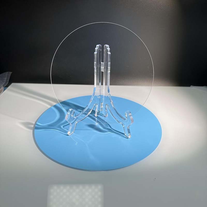
6inch HPSI SiC substrate wafer Silicon Carbide Semi-insulting SiC wafers


PVT Silicon Carbide Crystal SiC Growth Technology
The current growth methods for SiC single crystal mainly include the following three: liquid phase method, high temperature chemical vapour deposition method, and physical vapour phase transport (PVT) method. Among them, the PVT method is the most researched and mature technology for SiC single crystal growth, and its technical difficulties are:
(1) SiC single crystal in the high temperature of 2300 ° C above the closed graphite chamber to complete the "solid - gas - solid" conversion recrystallisation process, the growth cycle is long, difficult to control, and prone to microtubules, inclusions and other defects.
(2) Silicon carbide single crystal, including more than 200 different crystal types, but the production of general only one crystal type, easy to produce crystal type transformation in the growth process resulting in multi-type inclusions defects, the preparation process of a single specific crystal type is difficult to control the stability of the process, for example, the current mainstream of the 4H-type.
(3) Silicon carbide single crystal growth thermal field there is a temperature gradient, resulting in the crystal growth process there is a native internal stress and the resulting dislocations, faults and other defects induced.
(4) Silicon carbide single crystal growth process needs to strictly control the introduction of external impurities, so as to obtain a very high purity semi-insulating crystal or directionally doped conductive crystal. For the semi-insulating silicon carbide substrates used in RF devices, the electrical properties need to be achieved by controlling the very low impurity concentration and specific types of point defects in the crystal.
Detailed Diagram