4H-N Type SiC Epitaxial Wafer High Voltage High Frequency


Detailed Diagram


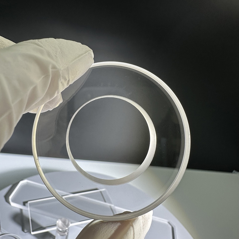
Overview
As industries move toward higher efficiency, compact power modules, and extreme condition operation, the SiC Epitaxial Wafer has emerged as a transformative material for next-generation semiconductors. The SiC Epitaxial Wafer, composed of an epitaxially grown layer of silicon carbide on a SiC substrate, enables unprecedented electrical and thermal performance. From high-voltage converters to smart grids, SiC Epitaxial Wafer technology is playing a pivotal role in reshaping the electronic landscape.
SiC Epitaxial Wafer structures are used to fabricate high-efficiency devices that can handle extreme voltages and currents while reducing energy loss and thermal stress. This makes the SiC Epitaxial Wafer indispensable for energy-critical applications.
Structure and Formation
The core concept of the SiC Epitaxial Wafer lies in its epitaxial growth—a method of depositing a crystalline layer that mimics the underlying substrate’s lattice structure. In the case of the SiC Epitaxial Wafer, this layer is typically doped with nitrogen or aluminum to create n-type or p-type conductivity profiles, depending on device requirements.
The manufacturing of a SiC Epitaxial Wafer generally involves:
-
Surface Cleaning: The SiC substrate is chemically and mechanically cleaned to eliminate contamination and ensure uniform deposition.
-
Epitaxial Growth: A low-defect silicon carbide layer is deposited using horizontal or vertical hot-wall CVD reactors under ultra-high purity conditions.
-
Precise Doping Control: By adjusting gas flow ratios of dopants like nitrogen (n-type) or aluminum (p-type), electrical characteristics of the SiC Epitaxial Wafer can be finely tailored.
-
Defect Suppression: Through process optimization, micropipes and dislocations within the SiC Epitaxial Wafer are minimized to improve device reliability.
SiC Epitaxial Wafer quality is measured through parameters such as carrier lifetime, resistivity uniformity, surface roughness, and basal plane dislocation (BPD) density.
Specification
| Parameter | Specification |
| Categories | Materials Science, Single Crystal Substrates |
| Polytype | 4H |
| Doping | N Type |
| Diameter | 101 mm |
| Diameter Tolerance | ± 5% |
| Thickness | 0.35 mm |
| Thickness Tolerance | ± 5% |
| Primary Flat Length | 22 mm (± 10%) |
| TTV (Total Thickness Variation) | ≤10 µm |
| Warp | ≤25 µm |
| FWHM | ≤30 Arc-sec |
| Surface Finish | Rq ≤0.35 nm |
Industrial Applications
The proliferation of the SiC Epitaxial Wafer in various industries demonstrates its strategic importance:
-
Traction Inverters in EVs: The use of SiC Epitaxial Wafer enables smaller, more efficient power converters, extending driving range.
-
High-Voltage DC Transmission: SiC Epitaxial Wafer components support 3.3kV to 15kV-class power modules with minimal losses.
-
Medical Equipment: High-reliability SiC Epitaxial Wafer-based semiconductors are found in MRI power supplies and diagnostic instruments.
-
Data Centers: Power regulation and cooling are significantly optimized using SiC Epitaxial Wafer technology.
-
Defense Radar Systems: Due to radiation hardness and fast switching capabilities, SiC Epitaxial Wafer materials are ideal for radar and satellite platforms.
Each SiC Epitaxial Wafer produced serves as a foundation for devices like MOSFETs, JFETs, Schottky diodes, and hybrid modules in high-efficiency systems.
Competitive Advantages
SiC Epitaxial Wafer technology holds several technological and commercial advantages over silicon and gallium arsenide alternatives:
-
Higher Electric Field Strength: SiC Epitaxial Wafer supports a critical field strength of ~3 MV/cm—significantly higher than silicon.
-
Wide Bandgap (~3.26 eV): Provides thermal stability, ideal for aerospace and automotive modules.
-
Reduced Cooling Requirements: Systems based on SiC Epitaxial Wafer generate less heat, reducing the need for heavy heat sinks.
-
Increased Efficiency: Lower on-resistance and leakage current help to reduce total system losses.
-
Miniaturization: Smaller components built with SiC Epitaxial Wafer enable lighter, denser system designs.
Moreover, lifecycle analysis shows that adopting SiC Epitaxial Wafer-based power systems can cut energy usage and emissions over the product lifespan.
Market Trends and Production Outlook
The demand for SiC Epitaxial Wafer products has seen exponential growth. As of recent industry projections, the global SiC Epitaxial Wafer market is expected to surpass $3 billion by 2028. With 6-inch and 8-inch wafer scaling becoming more common, manufacturers are investing in reactor capacity, in-situ monitoring, and AI-based quality control systems.
Additionally, vertical integration is becoming a key strategy—some device makers are now producing their own SiC Epitaxial Wafer to ensure material supply and consistency.
Frequently Asked Questions (FAQ)
Q1: Why choose SiC Epitaxial Wafer over conventional silicon wafers?
SiC Epitaxial Wafer provides higher thermal tolerance, higher voltage capability, and better energy efficiency in switching applications.
Q2: Are 8-inch SiC Epitaxial Wafers commercially available?
While 4-inch and 6-inch wafers are widely used, several manufacturers are piloting 8-inch SiC Epitaxial Wafer production for high-volume demand.
Q3: What are the typical thickness tolerances of the epitaxial layer?
Tolerance is usually ±1 μm for thin layers and up to ±5 μm for thicker layers, depending on the growth rate and reactor configuration.
Q4: How are defects detected in SiC Epitaxial Wafer?
Advanced metrology tools like KOH etching, XRD, and PL mapping are used to identify and quantify defects.
Q5: Can SiC Epitaxial Wafer be customized for specific resistivity and doping profiles?
Yes, custom SiC Epitaxial Wafer manufacturing supports a wide range of doping levels (from 1E14 to 1E19 cm⁻³) to suit various device designs.
Q6: What factors impact the price of a SiC Epitaxial Wafer?
The cost is influenced by substrate quality, epitaxial thickness, doping precision, and defect control technologies.
Q7: How is the supply chain evolving for SiC Epitaxial Wafer?
Major investments are being made globally in SiC crystal growth, substrate polishing, and epitaxy lines to scale production and reduce costs.
Related Products
-

GaAs laser epitaxial wafer 4 inch 6 inch VCSEL ...
-

99.999% Al2O3 sapphire boule monocrystal transp...
-

SiC Epitaxial Wafer for Power Devices – 4H-SiC,...
-

C/A/M axis 4 inch sapphire wafers single crysta...
-
Sapphire round washer ring hardness high wear r...
-

4inch Silicon wafer FZ CZ N-Type DSP or SSP Tes...