Semiconductor porous chucks precision ceramic vacuum chucks corrosion-resistant and high-temperature resistant


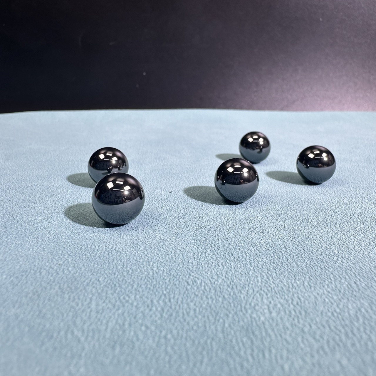
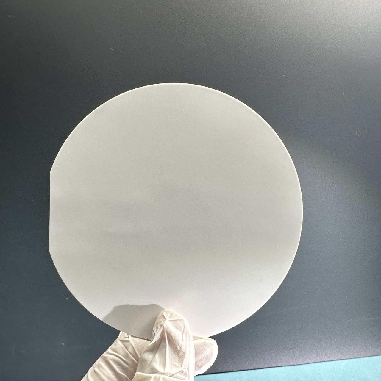
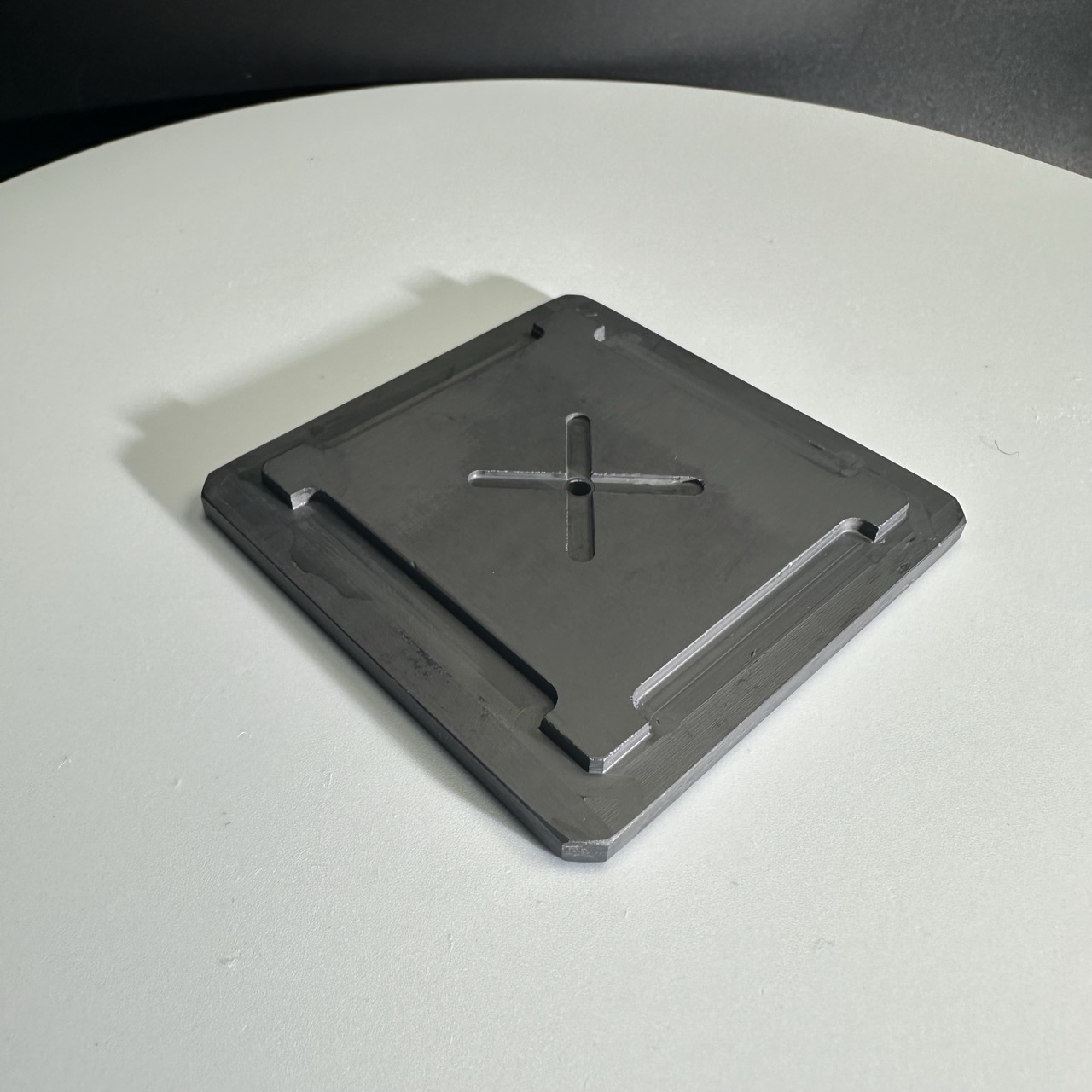
Detailed Diagram


Advantages
1. High Air-Tightness
With pore diameters of only 1–5 μm, gas must pass through the entire body of the material and encounters extremely high flow resistance — even at a pressure differential of 10 bar, no through-leakage occurs. The adsorption value is specified with a 35–40 bar design margin, so the workpiece stays firmly seated without drifting when the vacuum source fluctuates. The chuck contains no rubber O-rings, eliminating the slow leakage caused by seal ageing, hardening and particle shedding.
2. Corrosion & Wear Resistance
Made from chemically inert ceramic, the surface is unaffected by prolonged contact with acids, alkalis, cutting fluids, lapping slurries and deionized water. The SiC grade reaches a Vickers hardness of HV 2100 and HRA 94, so the pore size on the chuck surface remains stable even under continuous abrasive flushing. The material releases no metal ions, preventing metal contamination and ion migration on wafers.
3. Insulation / Anti-Static
The Al₂O₃ grade offers volume resistivity above 1×10¹⁰ Ω·cm, dielectric strength of 13–30 kV/mm and a dielectric constant of 9.5, making it a true insulator. The SiC grade, with resistivity of 1×10⁵–1×10⁸ Ω·cm, is anti-static — it does not accumulate surface charge or attract particles. With no exposed metal on the chuck surface, it can be used directly in electrically sensitive stations such as inspection, probing and plasma processes.
4. High Machining Accuracy
Flatness: 0.001–0.0015 mm for ceramic bases, 0.005–0.009 mm for stainless steel bases. Parallelism: 0.003–0.005 mm (ceramic) and 0.013–0.015 mm (stainless steel). Thickness tolerance is ±0.01 mm. The chuck surface can be polished, edges chamfered, and locating notches machined to drawing.
Porous Performance Parameters
| Classification | Material | Pore Size (μm) | Porosity | Pressure Difference (bar) | Adsorption Value (bar) | Electrical Resistivity (Ω·cm) | Color |
| Porous | Al₂O₃ | 1–5 | 15–30% | 10 | 35 | >1×10¹⁰ | White / Light Blue |
| Porous | Al₂O₃ | 50–100 | 15–40% | 8 | 40 | >1×10¹⁰ | White / Earthy Yellow / Dark Brown / Gray Black / Black |
| Porous | SiC | 20–50 | 30–50% | 10–20 | <−80 | >1×10⁵⁻⁸ | Lividity · Anti-Static |
| Porous | SiC | 50–100 | 30–50% | 30–40 | <−80 | >1×10⁵⁻⁸ | Lividity · Anti-Static |
Product Precision
| Classification | Specifications | Flatness | Parallelism | Operating Temperature |
| Stainless Steel + Porous | 6 inch | 0.005 | 0.013 | −40 ℃ ~ 80 ℃ |
| Stainless Steel + Porous | 8 inch | 0.007 | 0.015 | −40 ℃ ~ 80 ℃ |
| Stainless Steel + Porous | 12 inch | 0.009 | 0.015 | −40 ℃ ~ 80 ℃ |
| Ceramic + Porous | 6 inch | 0.001 | 0.003 | −40 ℃ ~ 80 ℃ |
| Ceramic + Porous | 8 inch | 0.001 | 0.003 | −40 ℃ ~ 80 ℃ |
| Ceramic + Porous | 12 inch | 0.0015 | 0.005 | −40 ℃ ~ 80 ℃ |
Typical Models
| Model | Application Field | Size Requirements | Accuracy Requirements | Material | Technical Advantage | Heat-Resistant |
| Dicing Chuck Table | Adsorption and fixation of wafers during the wafer dicing process | 4 / 6 / 8 / 12 inch | Flatness: 4 inch <2 μm · 6 inch <2 μm · 8 inch <3 μm · 12 inch <4 μm | Earthy yellow alumina ceramic suction cup + stainless steel base | Size φ250 × 30 mm. Flatness within 0.001, parallelism within 0.0027 | −40 ℃ ~ 80 ℃ |
| Spinning Chuck Table | Adsorption and fixation of wafers during dicing and back-lapping processes | 4 / 6 / 8 / 12 inch | Flatness: 4 inch <2 μm · 6 inch <2 μm · 8 inch <3 μm · 12 inch <4 μm | Gray black alumina ceramic suction cup + yellow alumina ceramic base | Size φ318 × 18 mm. Flatness within 0.0013, parallelism within 0.0047 | −40 ℃ ~ 80 ℃ |
| Wafer Dicing | Adsorption and fixation of wafers during the wafer dicing process | 4 / 6 / 8 / 12 inch | Flatness: 4 inch <2 μm · 6 inch <2 μm · 8 inch <3 μm · 12 inch <4 μm | Gray black alumina ceramic suction cup + stainless steel SUS630 base | Size φ330 × 15.66 mm. Flatness within 0.014, parallelism within 0.03 | −40 ℃ ~ 80 ℃ |
| Back Grinding Chuck Table | Back grinding of wafer backside | 4 / 6 / 8 / 12 inch | Flatness: 4 inch <2 μm · 6 inch <2 μm · 8 inch <3 μm · 12 inch <4 μm | Blue alumina ceramic suction cup + yellow alumina ceramic base | Size φ250 × 30 mm. Flatness within 0.002, parallelism within 0.003 | −40 ℃ ~ 80 ℃ |

Characteristics of Pan-Semiconductor Materials
Differences between wide-bandgap semiconductors and traditional silicon-based semiconductors mainly include:
1. Material Properties: Wide-bandgap semiconductor materials typically have a larger bandgap, making them well-suited for high-frequency, high-temperature, and high-power environments.
2. Application Scenarios: From 5G base stations to EV charging piles, wide-bandgap semiconductors deliver outstanding performance in new-generation infrastructure.
3. Manufacturing Processes: Some wide-bandgap semiconductor materials require special growth and processing techniques.

Material Property Comparison
| Property | Unit | A-100 (Al₂O₃ 96%) | A-200 (Al₂O₃ 99%) | A-300 (Al₂O₃ 99.7%) | A-600 (Al₂O₃ 99.9%) | Z-100 (ZrO₂-Y₂O₃) | ZM-200 (Mg-PSZ) | ZB-100 (ZrO₂-Y₂O₃) | SC-200 (SiC) | SN-200 (Si₃N₄) | SN-300 (Si₃N₄) | AlN |
| Density | g/cm³ | 3.60 | 3.88 | 3.91 | 3.92 | 6.00 | 5.70 | 6.00 | 3.15 | 3.20 | 3.20 | 3.30 |
| Flexural Strength | MPa | 310 | 360 | 400 | 400 | 900 | 600 | 900 | 400 | 700 | 950 | 320 |
| Compressive Strength | MPa | 2200 | 2250 | 2450 | 2240 | 2100 | 1600 | 2300 | 2000 | 3000 | 3800 | — |
| Young's Modulus | GPa | 300 | 330 | 380 | 380 | 200 | 210 | 220 | 430 | 290 | 300 | 220 |
| Fracture Toughness | MPa·m^1/2 | 3.5 | 3.5 | 4.0 | 4.0 | 7 | 7 | 6 | 4 | 6 | 7 | 7 |
| Vickers Hardness | HV1 | 1250 | 1450 | 1600 | 1600 | 1250 | 1200 | 1450 | 2100 | 1600 | 1650 | 1200 |
| Thermal Expansion α | 10⁻⁶/K | 7.2 | 7.1 | 6.8 | 6.8 | 11 | 9 | 10 | 3.5 | 3.2 | 3.2 | 4.5 |
| Thermal Conductivity | W/m·K | 24 | 25 | 32 | 32 | 3 | 3 | 3 | 90 | 30 | 30 | 180 |
| Thermal Shock Resistance | ΔT ℃ | 200 | 200 | 220 | 220 | 470 | 400 | 400 | 600 | 600 | 800 | — |
| Max Use Temp. in Air | ℃ | 1000 | 1000 | 1200 | 1200 | 1000 | 1000 | 1000 | 1350 | 1300 | 1300 | 1300 |
| Max Use Temp. in Vacuum / Inert | ℃ | 1000 | 1000 | 1400 | 1400 | 1000 | 850 | 1000 | 1350 | 1400 | 1400 | 2200 |
| Volume Resistivity | Ω·cm | 10¹⁴ | 10¹⁴ | 10¹⁵ | 10¹⁵ | 10¹³ | 5×10¹³ | 10¹² | 10⁵ | 10¹⁴ | 10¹⁴ | 10¹⁴ |
| Dielectric Strength | kV/mm | 13 | 16 | 20 | 30 | 19 | 19 | 17 | 0 | 15 | 19 | 14 |
| Dielectric Constant | 1 MHz | 9.5 | 9.5 | 9.5 | 9.5 | 28 | 27 | 30 | — | 9 | 9 | 8 |
| Dielectric Loss Tangent | tan δ | 3×10⁻⁴ | 3×10⁻³ | 1×10⁻⁴ | 1×10⁻⁴ | 2×10⁻³ | 2×10⁻³ (1 GHz) | 2×10⁻³ | — | 4×10⁻³ | 5×10⁻³ | 1×10⁻⁴ |
FAQ
Q1: What workpieces suit porous ceramic vacuum chucks?
Uniform negative pressure via interconnected micropores. Ideal for ultra-thin wafers, precision thin sheets and optical parts sensitive to local stress & back scratches. More even suction, less sheet deformation vs grooved chucks. Custom pore size, porosity, flatness and suction zones available at Fangtai New Materials.
Q2: Features & applications of grooved ceramic vacuum chucks
Groove air channels with large flow area for fast evacuation. For holding & positioning large, rigid workpieces. Check groove specs, sealing surface and vacuum ports to avoid concentrated suction stress.
Q3: Application of bump ceramic vacuum chucks
Workpieces supported by array bumps. Minimal contact area cuts backside contamination and particle adhesion, perfect for high backside cleanliness requirements. Tune bump parameters based on workpiece rigidity and thickness to avoid thin sheet sagging.