
Hello, everyone. Today we are going to talk about robotic arms used in semiconductor equipment.
When we talk about robotic arms, what do you think of first?Is it something like this?
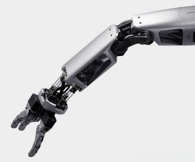
Or something like this?
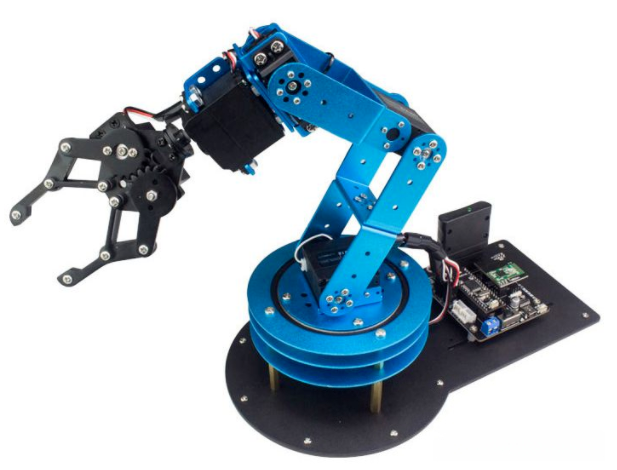
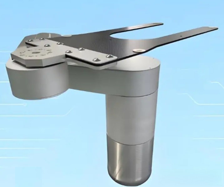
Actually, the robotic arms used in semiconductor equipment look like this.
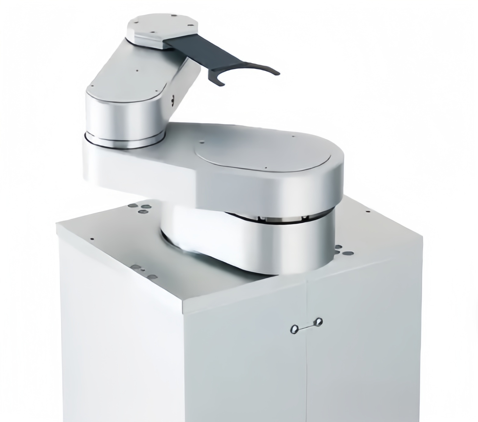
The semiconductor robotic arm is one of the important components of semiconductor equipment. It is mainly used to transfer, transport, and position semiconductor wafers, and is suitable for semiconductor front-end processes such as integrated circuit and chip manufacturing. It is used in grinding, polishing, etching, diffusion, deposition, assembly, packaging, and testing, among other processes.
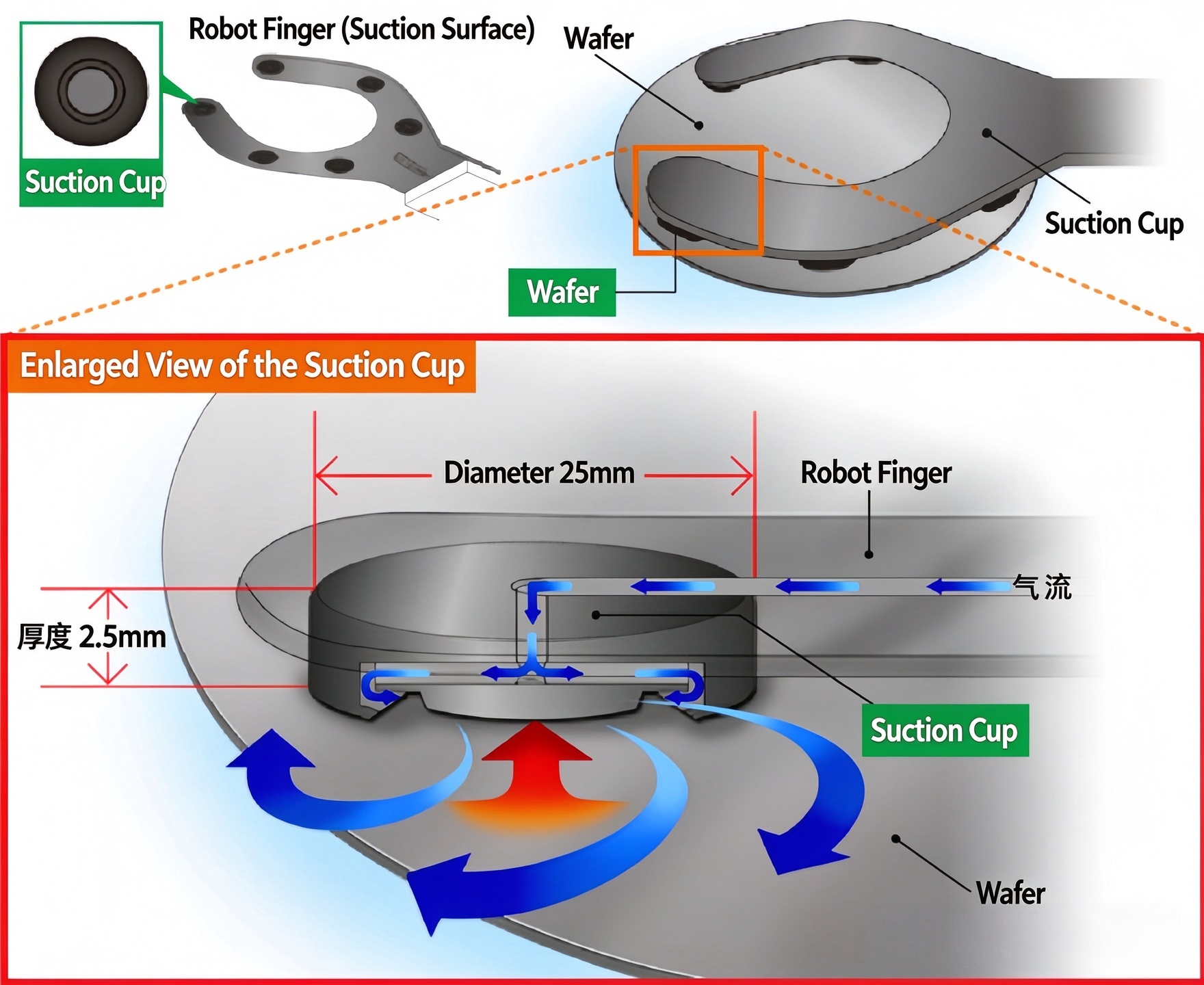
Semiconductor equipment robotic arms pick up wafers by vacuum suction—that is, using the suction-cup principle to adsorb the semiconductor wafer onto quartz or ceramic fingers, and then transport the wafer through the robotic arm’s extension/retraction, rotation, and lifting movements.
“High speed” and “cleanliness” are the core characteristics of semiconductor wafer handling equipment. To meet these characteristics, the performance requirements for the components used in the equipment are extremely stringent. Because many processes are carried out in vacuum, high-temperature, and corrosive gas environments, the handling arms used in the equipment must have excellent physical properties, such as high mechanical strength, corrosion resistance, high-temperature resistance, wear resistance, high hardness, and insulation.
Based on these strict requirements, in vacuum environments, robotic arms made of most other materials cannot meet the requirements. Therefore, ceramic arms with high-temperature resistance, wear resistance, and high hardness are needed.
Advantages of ceramic robotic arms:
1.Ceramic robotic arms are more resistant to acid and alkali corrosion. They have a longer service life in various semiconductor processes.
2.Ceramic robotic arms are not likely to react with other substances. They do not leave polluting fine particles or charged particles on contacted objects, do not produce metal ions, and do not contaminate semiconductor parts.
3.During heat treatment of semiconductors, ceramic robotic arms undergo little thermal deformation, reducing the deformation of semiconductor parts during heat treatment.
Materials of ceramic robotic arms:
Usually, high-purity alumina and silicon carbide are used to make ceramic arms. Both raw materials have physical properties such as high hardness, good wear resistance, and good high-temperature resistance, making them excellent materials for ceramic arms.
(1) Alumina can be used to make most semiconductor ceramic components. Depending on its content, the performance of the resulting products also differs. Alumina ceramic components with a purity of 95% are light yellow, while alumina ceramic products with a purity of 99% are snow white. They have excellent stiffness, strength, toughness, high-temperature resistance, corrosion resistance, and plasma erosion resistance.
(2) Silicon carbide ceramics are black. They have relatively high thermal conductivity, high strength, high hardness, resistance to deformation, good shock resistance, and also high-temperature and corrosion resistance. Compared with alumina ceramics, they are lighter in weight.
Compared with alumina ceramics, ceramic arms made of silicon carbide have better performance. However, considering material price and processing difficulty, alumina ceramic arms are more cost-effective, and alumina ceramic arms are usually used more often.
Principle of ceramic robotic arms:
Bernoulli principle: The gas introduced through the supply port is ejected at high speed from the nozzles on the inner cylindrical side of the chuck and forms a swirling airflow in the cylindrical space inside the chuck, creating negative pressure. The airflow is finally released to the outside through the gap between the robotic finger’s suction surface and the wafer surface. The airflow forms a stable laminar flow in the space between the vortex chuck and the wafer and creates a pressure difference between the upper and lower surfaces of the wafer, ultimately generating an upward suction force on the wafer.
According to different working environments, robotic arms can be divided into two types: vacuum robotic arms and atmospheric robotic arms. Vacuum robotic arms are used for wafer handling in environments with a vacuum degree of 10⁻⁵ Pa. This type of robotic arm is mostly used in cluster tools and completes wafer transfer and positioning through trajectory planning. The other type is the atmospheric robotic arm, which is used in a clean atmospheric environment. Such robotic arms have relatively high docking accuracy requirements—generally Grade 10, with some reaching Grade 1. According to QYR data, atmospheric robotic arms are currently the most widely used, accounting for nearly 60% of the semiconductor robotic arm market.
By region, manufacturers in the United States and Japan dominate the production of semiconductor robotic arms. Japan is the world’s largest production region for semiconductor robotic arms, accounting for about 60% of the market share; the United States accounts for about 20%; and South Korea is also an important production region, accounting for about 6%. Domestic Chinese manufacturers mainly include Shenyang Siasun Robot, Huazhuo Jingke, Xiayang New Materials, Hunan Shengci, Fangtai New Materials, etc.
Post time: Nov-09-2026