
300mm Sapphire Wafer Technology: Material Stability and Precision Engineering for Semiconductor Applications
Introduction
The semiconductor industry continues to advance toward more sophisticated chip architectures, higher integration density, and improved computing performance. The growth of AI computing, data-center processors, and advanced heterogeneous integration has increased interest in precision materials and specialized wafer-level components.
Technologies such as CoWoS-L demonstrate the industry’s move toward integrating multiple logic dies, chiplets, and high-bandwidth memory within increasingly complex packages. As advanced packaging evolves, material selection and process engineering remain important considerations in research, equipment development, and supporting manufacturing operations.
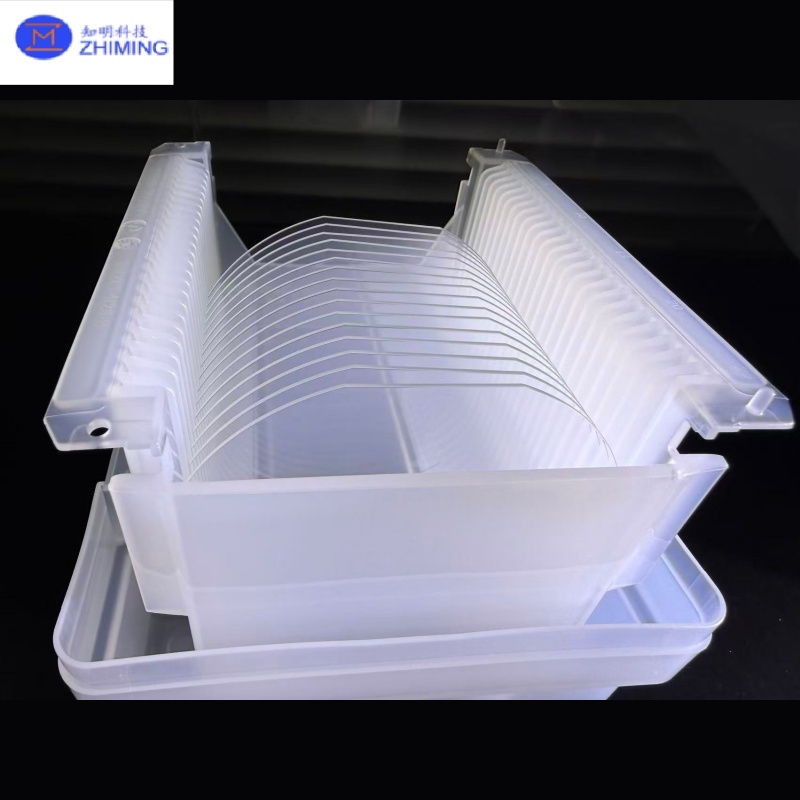
In this environment, 300 mm sapphire wafers offer a specialized material platform for applications that benefit from the distinctive properties of single-crystal aluminum oxide.
Sapphire: A High-Performance Engineering Material
Sapphire is a single-crystal form of aluminum oxide (Al₂O₃). Its combination of high hardness, chemical resistance, and thermal stability makes it suitable for a variety of demanding industrial and scientific applications.
Unlike conventional silicon wafers, sapphire is electrically insulating under normal conditions and has different thermal expansion, surface, and processing characteristics. These differences can be advantageous in selected optical, dielectric, and materials research applications, although they also require careful evaluation when integrating sapphire into semiconductor manufacturing equipment or process flows.
Sapphire’s optical transmission depends on wavelength, crystal quality, thickness, and surface finish. This makes material selection and polishing specifications particularly important when optical performance is part of the intended application.
Advantages of a 12-Inch Sapphire Substrate
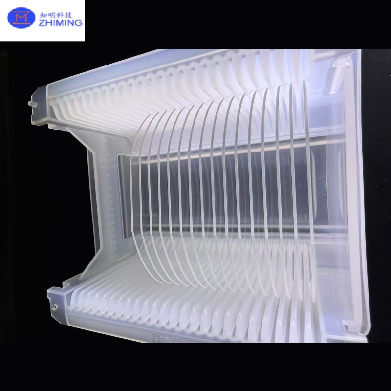 A 12-inch sapphire substrate offers a nominal 300 mm diameter format for projects requiring a large-area crystalline material. Depending on the application, key considerations include:
Mechanical durability: Sapphire’s high hardness provides strong resistance to scratching, supporting applications that require a durable surface.
Chemical stability: Sapphire resists many chemicals, although compatibility should always be verified for the specific etchants, cleaning agents, and process conditions involved.
Surface precision: Controlled polishing and dimensional tolerances can support research projects that require consistent surface quality and reproducible wafer geometry.
Customized configurations: Thickness, crystal orientation, surface finish, and edge geometry can be specified according to manufacturing capabilities and customer requirements.
These features make customized sapphire wafers worth evaluating for selected thin-film studies, optical systems, specialized fixtures, and other semiconductor-related research applications.
Connection with CoWoS-L and Advanced Packaging
CoWoS-L combines an RDL-based interposer with embedded local silicon interconnects to support high-density connections between dies. It is an advanced packaging architecture developed for demanding applications, including high-performance computing and AI systems.
Although sapphire is not a standard functional interconnect material in CoWoS-L, a 300 mm sapphire wafer may be investigated for separate supporting applications in the broader semiconductor ecosystem. Examples could include customized process-development platforms, optical inspection components, or specialized fixtures, provided the design and process requirements are compatible with sapphire.
Such applications require technical validation. Factors including coefficient of thermal expansion, thermal conductivity, electrical behavior, wafer handling, bonding methods, and surface cleanliness should be assessed before a sapphire component is introduced into a specific manufacturing environment.
Precision Manufacturing and Quality Control
For large-diameter sapphire wafers, consistent manufacturing quality is essential. Important inspection parameters may include diameter, thickness, total thickness variation (TTV), flatness, surface roughness, crystal orientation, edge condition, and surface defects.
The appropriate specifications depend on the intended use. A wafer for optical applications may require different surface and transmission characteristics from one designed for thin-film research or a specialized process fixture.
By matching material properties with application-specific tolerances, manufacturers can provide sapphire substrates better suited to the technical demands of each project.
Customized 300mm Sapphire Wafer Solutions
As semiconductor manufacturing continues to explore new packaging architectures and specialized process materials, customized sapphire substrates remain a useful option for selected applications that require a combination of mechanical durability, chemical stability, and controlled surface quality.
Our 12-inch sapphire substrates can be tailored to project-specific requirements, including thickness, crystal orientation, polishing method, and dimensional tolerances, subject to manufacturing capability.
Whether your project involves optical components, thin-film research, wafer-level material evaluation, or supporting studies related to advanced packaging technologies such as CoWoS-L, our team can help evaluate suitable sapphire wafer configurations.
Contact us to discuss your 300 mm sapphire wafer requirements and identify specifications aligned with your application.
Post time: Oct-29-2026