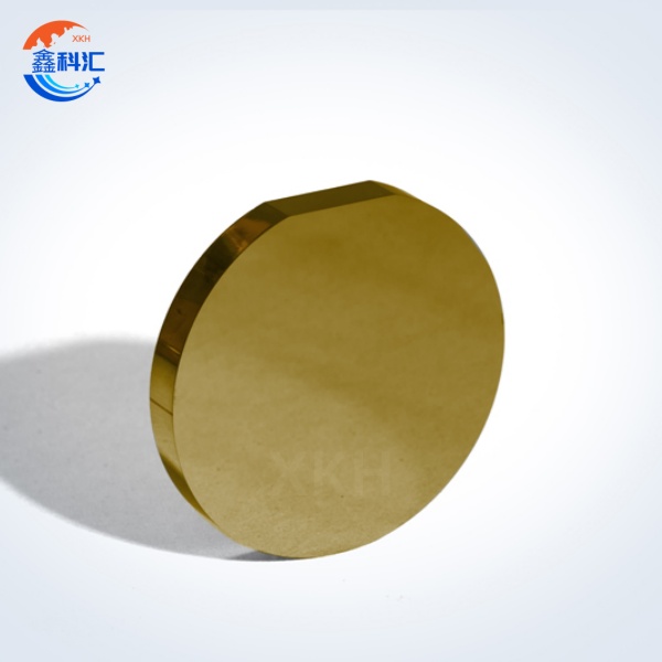
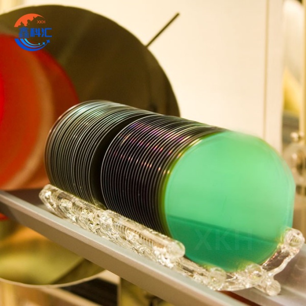
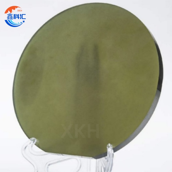
12 Inch SiC substrate Diameter 300mm Thickness 750μm 4H-N Type can be customized


Technical parameters
| 12 inch Silicon Carbide (SiC) Substrate Specification | |||||
| Grade | ZeroMPD Production Grade(Z Grade) |
Standard Production Grade(P Grade) |
Dummy Grade (D Grade) |
||
| Diameter | 3 0 0 mm~1305mm | ||||
| Thickness | 4H-N | 750μm±15 μm | 750μm±25 μm | ||
| 4H-SI | 750μm±15 μm | 750μm±25 μm | |||
| Wafer Orientation | Off axis : 4.0° toward <1120 >±0.5° for 4H-N, On axis : <0001>±0.5° for 4H-SI | ||||
| Micropipe Density | 4H-N | ≤0.4cm-2 | ≤4cm-2 | ≤25cm-2 | |
| 4H-SI | ≤5cm-2 | ≤10cm-2 | ≤25cm-2 | ||
| Resistivity | 4H-N | 0.015~0.024 Ω·cm | 0.015~0.028 Ω·cm | ||
| 4H-SI | ≥1E10 Ω·cm | ≥1E5 Ω·cm | |||
| Primary Flat Orientation | {10-10} ±5.0° | ||||
| Primary Flat Length | 4H-N | N/A | |||
| 4H-SI | Notch | ||||
| Edge Exclusion | 3 mm | ||||
| LTV/TTV/Bow /Warp | ≤5μm/≤15μm/≤35 μm/≤55 μm | ≤5μm/≤15μm/≤35 □ μm/≤55 □ μm | |||
| Roughness | Polish Ra≤1 nm | ||||
| CMP Ra≤0.2 nm | Ra≤0.5 nm | ||||
| Edge Cracks By High Intensity Light Hex Plates By High Intensity Light Polytype Areas By High Intensity Light Visual Carbon Inclusions Silicon Surface Scratches By High Intensity Light |
None Cumulative area ≤0.05% None Cumulative area ≤0.05% None |
Cumulative length ≤ 20 mm, single length≤2 mm Cumulative area ≤0.1% Cumulative area≤3% Cumulative area ≤3% Cumulative length≤1×wafer diameter |
|||
| Edge Chips By High Intensity Light | None permitted ≥0.2mm width and depth | 7 allowed, ≤1 mm each | |||
| (TSD) Threading screw dislocation | ≤500 cm-2 | N/A | |||
| (BPD) Base plane dislocation | ≤1000 cm-2 | N/A | |||
| Silicon Surface Contamination By High Intensity Light | None | ||||
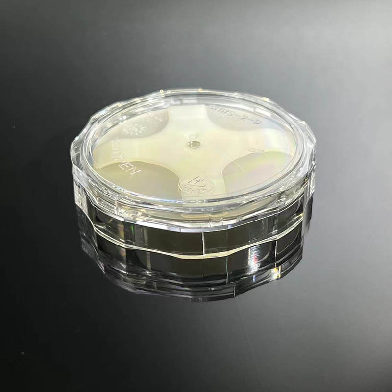
| Packaging | Multi-wafer Cassette Or Single Wafer Container | ||||
| Notes: | |||||
| 1 Defects limits apply to entire wafer surface except for the edge exclusion area. 2The scratches should be checked on Si face only. 3 The dislocation data is only from KOH etched wafers. |
|||||
Key Features
1.Production Capacity and Cost Advantages: The mass production of 12-inch SiC substrate (12-inch silicon carbide substrate) marks a new era in semiconductor manufacturing. The number of chips obtainable from a single wafer reaches 2.25 times that of 8-inch substrates, directly driving a leap in production efficiency. Customer feedback indicates that adopting 12-inch substrates has reduced their power module production costs by 28%, creating a decisive competitive advantage in the fiercely contested market.
2.Outstanding Physical Properties: The 12-inch SiC substrate inherits all advantages of silicon carbide material - its thermal conductivity is 3 times that of silicon, while its breakdown field strength reaches 10 times that of silicon. These characteristics enable devices based on 12-inch substrates to operate stably in high-temperature environments exceeding 200°C, making them particularly suitable for demanding applications such as electric vehicles.
3.Surface Treatment Technology: We have developed a novel chemical mechanical polishing (CMP) process specifically for 12-inch SiC substrates, achieving atomic-level surface flatness (Ra<0.15nm). This breakthrough solves the worldwide challenge of large-diameter silicon carbide wafer surface treatment, clearing obstacles for high-quality epitaxial growth.
4.Thermal Management Performance: In practical applications, 12-inch SiC substrates demonstrate remarkable heat dissipation capabilities. Test data shows that under the same power density, devices using 12-inch substrates operate at temperatures 40-50°C lower than silicon-based devices, significantly extending equipment service life.
Main Applications
1.New Energy Vehicle Ecosystem: The 12-inch SiC substrate (12-inch silicon carbide substrate) is revolutionizing electric vehicle powertrain architecture. From onboard chargers (OBC) to main drive inverters and battery management systems, the efficiency improvements brought by 12-inch substrates increase vehicle range by 5-8%. Reports from a leading automaker indicate that adopting our 12-inch substrates reduced energy loss in their fast-charging system by an impressive 62%.
2.Renewable Energy Sector: In photovoltaic power stations, inverters based on 12-inch SiC substrates not only feature smaller form factors but also achieve conversion efficiency exceeding 99%. Particularly in distributed generation scenarios, this high efficiency translates to annual savings of hundreds of thousands of yuan in electricity losses for operators.
3.Industrial Automation: Frequency converters utilizing 12-inch substrates demonstrate excellent performance in industrial robots, CNC machine tools, and other equipment. Their high-frequency switching characteristics improve motor response speed by 30% while reducing electromagnetic interference to one-third of conventional solutions.
4.Consumer Electronics Innovation: Next-generation smartphone fast-charging technologies have begun adopting 12-inch SiC substrates. It is projected that fast-charging products above 65W will fully transition to silicon carbide solutions, with 12-inch substrates emerging as the optimal cost-performance choice.
XKH Customized Services for 12-inch SiC Substrate
To meet specific requirements for 12-inch SiC substrates (12-inch silicon carbide substrates), XKH offers comprehensive service support:
1.Thickness Customization:
We provide 12-inch substrates in various thickness specifications including 725μm to meet different application needs.
2.Doping concentration:
Our manufacturing supports multiple conductivity types including n-type and p-type substrates, with precise resistivity control in the range of 0.01-0.02Ω·cm.
3.Testing Services:
With complete wafer-level testing equipment, we provide full inspection reports.
XKH understands that each customer has unique requirements for 12-inch SiC substrates. We therefore offer flexible business cooperation models to provide the most competitive solutions, whether for:
· R&D samples
· Volume production purchases
Our customized services ensure we can meet your specific technical and production needs for 12-inch SiC substrates.
Related Products
-

4inch 6inch 8inch SiC Crystal Growth Furnace fo...
-

As-grown sapphire boule ingot crystal ky method
-

Customized Sapphire Glass Windows Sapphire Opti...
-

Lens Prism Optical Glass DSP Custom Size 99.999...
-

Ultrafast Laser Rainbow Marking Machine Metal I...
-
2inch 50.8mm single wafer carrier box of PC and PP