Semiconductor Laser Lift-Off Equipment Revolutionize Ingot Thinning


Detailed Diagram
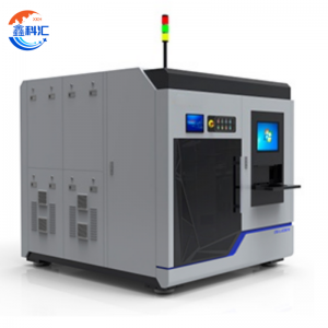
Product Introduction of Semiconductor Laser Lift-Off Equipment
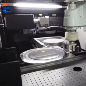
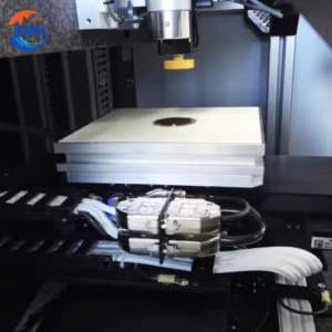
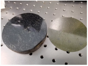
The Semiconductor Laser Lift-Off Equipment is a highly specialized industrial solution engineered for precise and non-contact thinning of semiconductor ingots through laser-induced lift-off techniques. This advanced system plays a pivotal role in modern semiconductor wafering processes, especially in the fabrication of ultra-thin wafers for high-performance power electronics, LEDs, and RF devices. By enabling the separation of thin layers from bulk ingots or donor substrates, Semiconductor Laser Lift-Off Equipment revolutionizes ingot thinning by eliminating mechanical sawing, grinding, and chemical etching steps.
Traditional thinning of semiconductor ingots, such as gallium nitride (GaN), silicon carbide (SiC), and sapphire, is often labor-intensive, wasteful, and prone to microcracks or surface damage. In contrast, Semiconductor Laser Lift-Off Equipment offers a non-destructive, precise alternative that minimizes material loss and surface stress while increasing productivity. It supports a wide variety of crystalline and compound materials and can be seamlessly integrated into front-end or midstream semiconductor production lines.
With configurable laser wavelengths, adaptive focus systems, and vacuum-compatible wafer chucks, this equipment is particularly well-suited for ingot slicing, lamella creation, and ultra-thin film detachment for vertical device structures or heteroepitaxial layer transfer.
Parameter of Semiconductor Laser Lift-Off Equipment
| Wavelength | IR/SHG/THG/FHG |
|---|---|
| Pulse Width | Nanosecond, Picosecond, Femtosecond |
| Optical System | Fixed optical system or Galvano-optical system |
| XY Stage | 500 mm × 500 mm |
| Processing Range | 160 mm |
| Movement Speed | Max 1,000 mm/sec |
| Repeatability | ±1 μm or less |
| Absolute Position Accuracy: | ±5 μm or less |
| Wafer Size | 2–6 inches or customized |
| Control | Windows 10,11 and PLC |
| Power Supply Voltage | AC 200 V ±20 V, Single-phase, 50/60 kHz |
| External Dimensions | 2400 mm (W) × 1700 mm (D) × 2000 mm (H) |
| Weight | 1,000 kg |
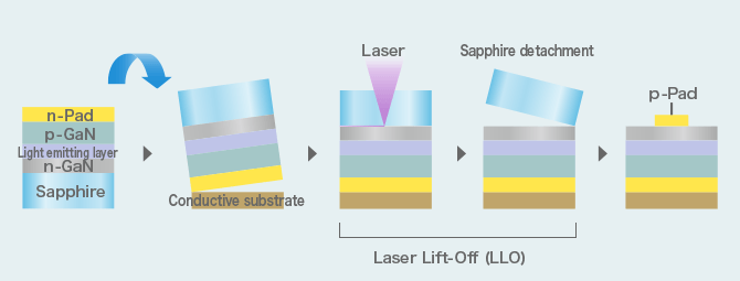
Working Principle of Semiconductor Laser Lift-Off Equipment
The core mechanism of the Semiconductor Laser Lift-Off Equipment relies on selective photothermal decomposition or ablation at the interface between the donor ingot and the epitaxial or target layer. A high-energy UV laser (typically KrF at 248 nm or solid-state UV lasers around 355 nm) is focused through a transparent or semi-transparent donor material, where the energy is selectively absorbed at a predetermined depth.
This localized energy absorption creates a high-pressure gas phase or thermal expansion layer at the interface, which initiates the clean delamination of the upper wafer or device layer from the ingot base. The process is finely tuned by adjusting parameters such as pulse width, laser fluence, scanning speed, and z-axis focal depth. The result is an ultra-thin slice—often in the 10 to 50 µm range—cleanly separated from the parent ingot without mechanical abrasion.
This method of laser lift-off for ingot thinning avoids the kerf loss and surface damage associated with diamond wire sawing or mechanical lapping. It also preserves crystal integrity and reduces downstream polishing requirements, making Semiconductor Laser Lift-Off Equipment a game-changing tool for next-generation wafer production.
Applications of Semiconductor Laser Lift-Off Equipment
Semiconductor Laser Lift-Off Equipment finds wide applicability in ingot thinning across a range of advanced materials and device types, including:
-
GaN and GaAs Ingot Thinning for Power Devices
Enables thin wafer creation for high-efficiency, low-resistance power transistors and diodes.
-
SiC Substrate Reclamation and Lamella Separation
Allows wafer-scale lift-off from bulk SiC substrates for vertical device structures and wafer reuse.
-
LED Wafer Slicing
Facilitates lift-off of GaN layers from thick sapphire ingots to produce ultra-thin LED substrates.
-
RF and Microwave Device Fabrication
Supports ultra-thin high-electron-mobility transistor (HEMT) structures needed in 5G and radar systems.
-
Epitaxial Layer Transfer
Precisely detaches epitaxial layers from crystalline ingots for reuse or integration into heterostructures.
-
Thin-Film Solar Cells and Photovoltaics
Used to separate thin absorber layers for flexible or high-efficiency solar cells.
In each of these domains, Semiconductor Laser Lift-Off Equipment provides unmatched control over thickness uniformity, surface quality, and layer integrity.
Advantages of Laser-Based Ingot Thinning
-
Zero-Kerf Material Loss
Compared to traditional wafer slicing methods, the laser process results in nearly 100% material utilization.
-
Minimal Stress and Warping
Non-contact lift-off eliminates mechanical vibration, reducing wafer bow and microcrack formation.
-
Surface Quality Preservation
No post-thinning lapping or polishing required in many cases, as laser lift-off preserves top-surface integrity.
-
High Throughput and Automation Ready
Capable of processing hundreds of substrates per shift with automated loading/unloading.
-
Adaptable to Multiple Materials
Compatible with GaN, SiC, sapphire, GaAs, and emerging III-V materials.
-
Environmentally Safer
Reduces use of abrasives and harsh chemicals typical in slurry-based thinning processes.
-
Substrate Reuse
Donor ingots can be recycled for multiple lift-off cycles, greatly reducing material costs.
Frequently Asked Questions (FAQ) of Semiconductor Laser Lift-Off Equipment
-
Q1: What thickness range can the Semiconductor Laser Lift-Off Equipment achieve for wafer slices?
A1: Typical slice thickness ranges from 10 µm to 100 µm depending on the material and configuration.Q2: Can this equipment be used to thin ingots made of opaque materials like SiC?
A2: Yes. By tuning the laser wavelength and optimizing interface engineering (e.g., sacrificial interlayers), even partially opaque materials can be processed.Q3: How is the donor substrate aligned before laser lift-off?
A3: The system uses sub-micron vision-based alignment modules with feedback from fiducial marks and surface reflectivity scans.Q4: What is the expected cycle time for one laser lift-off operation?
A4: Depending on wafer size and thickness, typical cycles last from 2 to 10 minutes.Q5: Does the process require a cleanroom environment?
A5: While not mandatory, cleanroom integration is recommended to maintain substrate cleanliness and device yield during high-precision operations.
About Us
XKH specializes in high-tech development, production, and sales of special optical glass and new crystal materials. Our products serve optical electronics, consumer electronics, and the military. We offer Sapphire optical components, mobile phone lens covers, Ceramics, LT, Silicon Carbide SIC, Quartz, and semiconductor crystal wafers. With skilled expertise and cutting-edge equipment, we excel in non-standard product processing, aiming to be a leading optoelectronic materials high-tech enterprise.
Related Products
-

8 inch SiC silicon carbide wafer 4H-N type 0.5m...
-
High hardness translucent sapphire single cryst...
-

8inch LNOI (LiNbO3 on Insulator) Wafer for Opti...
-

Alumina ceramic arm custom Ceramic robotic arm
-

Sapphire hair transplant blade high hardness co...
-

Silicon carbide ceramic tray sucker Silicon car...