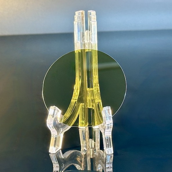
8inch 200mm Silicon Carbide SiC Wafers 4H-N type Production grade 500um thickness


200mm 8inch SiC Substrate Specification
Size: 8inch;
Diameter: 200mm±0.2;
Thickness: 500um±25;
Surface Orientation: 4 toward [11-20]±0.5°;
Notch orientation:[1-100]±1°;
Notch depth: 1±0.25mm;
Micropipe: <1cm2;
Hex Plates: None Permitted;
Resistivity: 0.015~0.028Ω;
EPD:<8000cm2;
TED:<6000cm2
BPD:<2000cm2
TSD:<1000cm2
SF: area<1%
TTV≤15um;
Warp≤40um;
Bow≤25um;
Poly areas: ≤5%;
Scratch: <5 and Cumulative Length< 1 Wafer Diameter;
Chips/Indents: None permit D>0.5mm Width and Depth;
Cracks: None;
Stain: None
Wafer edge: Chamfer;
Surface finish: Double Side Polish, Si Face CMP;
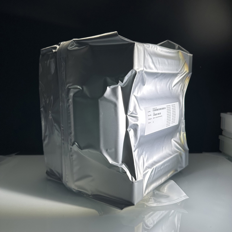
Packing: Multi-wafer Cassette Or Single Wafer Container;
The current difficulties in the preparation of 200mm 4H-SiC crystals mainl
1) The preparation of high-quality 200mm 4H-SiC seed crystals;
2) Large size temperature field non-uniformity and nucleation process control;
3) The transport efficiency and evolution of gaseous components in largeize crystal growth systems;
4) Crystal cracking and defect proliferation caused by large size thermal stress increase.
To overcome these challenges and obtain high quality 200mm SiC waferssolutions are proposed:
In terms of 200mm seed crystal preparation, appropriate temperature fieldflow field, and expanding assembly were studied and designed to take intoaccount crystal quality and expanding size; Starting with a 150mm SiC se:d crystal, carry out seed crystal iteration to gradually expand the SiC crystasize until it reaches 200mm; Through multiple crystal growth and processiig, gradually optimize the crystal quality in the crystal expanding area, andimprove the quality of 200mm seed crystals.
In terms of 200mm conductive crystal and substrate preparation, research has optimized the temperature feld and flow field design for large size crystalgrowth, conduct 200mm conductive SiC crystal growth, and control doping uniformity. After rough processing and shaping of the crystal, an 8-inchelectricaly conductive 4H-SiC ingot with a standard diameter was obtained. After cutting, grinding, polishing, processing to obtain SiC 200mm waferswith a thickness of 525um or so
Detailed Diagram