Semiconductor Ion Implantation Equipment

Detailed Diagram

Semiconductor Ion Implantation Equipment
Ai300 Medium Beam Ion Implanter (12-inch)
(1) Product Overview
The Ai300 is a medium beam ion implantation system designed for 12-inch wafer processing in advanced semiconductor manufacturing. It is primarily used for medium-dose and medium-to-high energy implantation steps, including well formation, channel engineering, and lightly doped drain (LDD) structures in CMOS processes. The system provides precise control of dopant depth and concentration profiles through stable beam delivery and accurate angle control, enabling optimization of device electrical characteristics.
(2) Key Specifications
- Wafer size: 12 inch
- Energy range: 5–300 keV
- Implant species: C, B, P, N, He, Ar
- Implant angle: 0°–45° (accuracy ≤0.1°)
- Dose range: 1E11–1E16 ions/cm²
- Beam stability: ≤10%/hour
- Beam parallelism: ≤0.1°
- Throughput: ≥500 WPH
- Uniformity/Repeatability: ≤0.5%
(3) Technical Features and Advantages
The Ai300 integrates a high-stability ion source and advanced beam control system, ensuring minimal beam fluctuation during extended operation. Its excellent beam parallelism guarantees uniform dopant distribution across the wafer, which is critical for advanced nodes. In addition, its high throughput supports high-volume manufacturing (HVM) requirements in 12-inch fabs.
(4) Applications
- Advanced logic devices (CMOS, FinFET)
- DRAM and NAND memory
- Precision doping processes
FAQ
1. What is ion implantation and why is it important in semiconductor manufacturing?
Ion implantation is a process in which dopant ions are accelerated and implanted into a semiconductor substrate to modify its electrical properties. Compared with traditional diffusion methods, ion implantation offers precise control over dopant concentration, depth, and lateral distribution, making it indispensable for advanced semiconductor device fabrication.
2. What is the difference between medium beam and high beam ion implanters?
Medium beam implanters are typically used for precision doping applications with moderate dose and wider energy ranges, such as well formation and channel engineering.
High beam implanters, on the other hand, are optimized for high-dose implantation with higher beam currents, commonly used for source/drain formation and contact engineering.
3. How do I choose the right ion implantation system for my process?
The selection depends on several key factors:
- Dose requirement (low/medium vs high dose)
- Energy range (shallow vs deep junction)
- Wafer size (6/8 inch vs 12 inch)
- Material type (Si vs SiC)
For example:
- Use Ai300 for advanced CMOS precision doping
- Use Ai80HC for high-dose source/drain processes
- Use Ai350HT for SiC high-temperature implantation
About Us
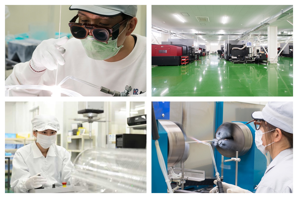
XKH specializes in high-tech development, production, and sales of special optical glass and new crystal materials. Our products serve optical electronics, consumer electronics, and the military. We offer Sapphire optical components, mobile phone lens covers, Ceramics, LT, Silicon Carbide SIC, Quartz, and semiconductor crystal wafers. With skilled expertise and cutting-edge equipment, we excel in non-standard product processing, aiming to be a leading optoelectronic materials high-tech enterprise.
Related Products
-
Sapphire Corundum for Gemstone Al2O3 crystal ru...
-

Ruby optics Ruby rod optical window titanium ge...
-

Fiber Laser Marking Ultra-Fine Marking for Jewe...
-

Gallium Nitride (GaN) Epitaxial Grown on Sapphi...
-
FZ CZ Si wafer in stock 12inch Silicon wafer Pr...
-

Al2O3 sapphire tube,Sapphire Capillary tube,R...