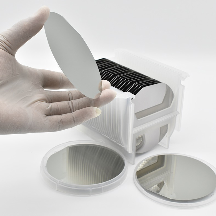
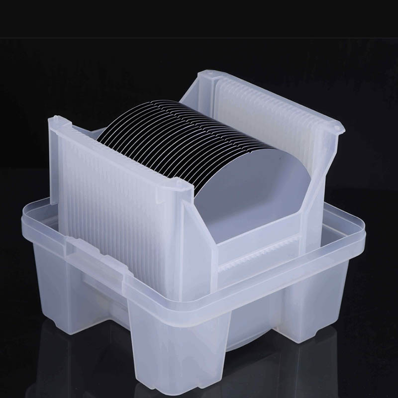
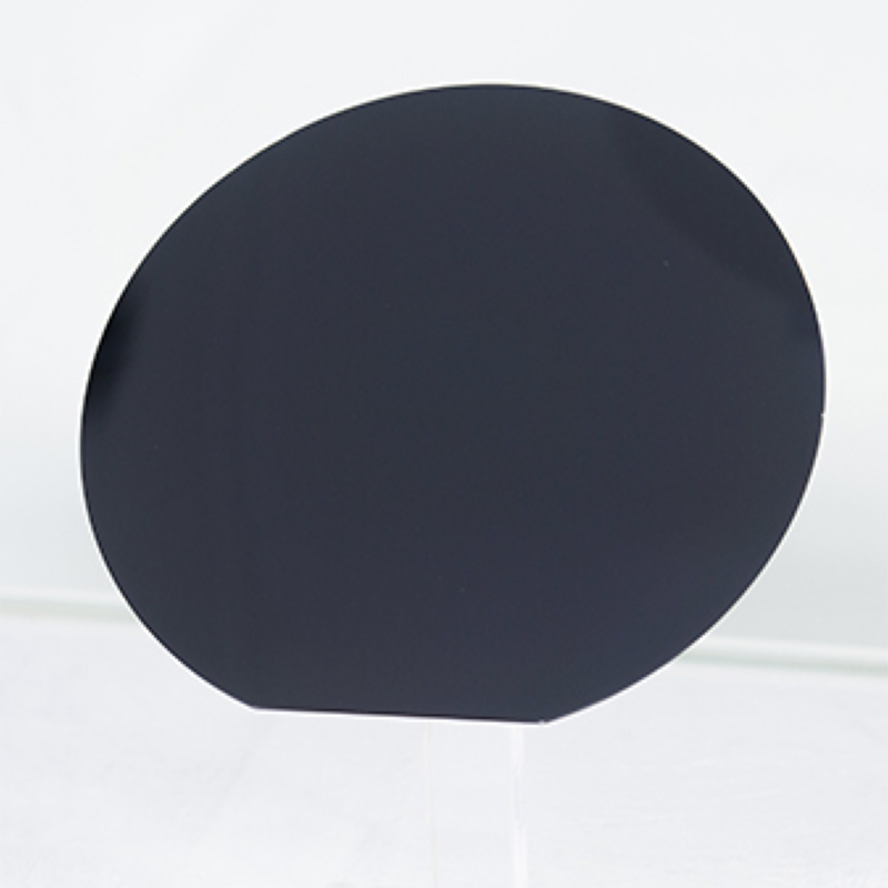
8-Inch Silicon Carbide Epitaxial Wafer (SiC Epi Wafer)


Detailed Diagram


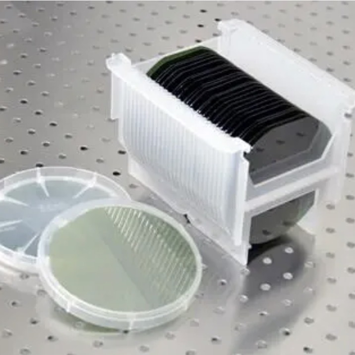
Product Overview of SiC EPI wafer
The 8-inch Silicon Carbide (SiC) epitaxial wafer is a high-performance semiconductor material designed for next-generation power electronics. Built on high-quality 8-inch SiC substrates, the epitaxial layer is grown using advanced chemical vapor deposition (CVD) technology to achieve precise thickness, doping control, and superior crystal quality.
Compared with traditional silicon wafers, SiC epitaxial wafers offer outstanding electrical, thermal, and mechanical properties, making them ideal for high-voltage, high-frequency, and high-temperature applications.


Working Principle of SiC EPI wafer
The SiC epitaxial layer is deposited on a polished SiC substrate through a high-temperature CVD process. During growth:
- Silicon- and carbon-containing gases react at elevated temperatures
- A single-crystal SiC layer is formed following the substrate lattice
- Doping gases (N-type or P-type) are introduced to control electrical properties
This epitaxial layer serves as the active region for device fabrication, enabling precise control of device performance such as breakdown voltage and on-resistance.
Key Features
- Large Diameter (8-inch / 200 mm): Supports high-volume manufacturing and cost reduction
- Low Defect Density: Minimizes micropipes and dislocations
- Excellent Thickness Uniformity: Ensures consistent device performance
- Precise Doping Control: Supports customized electrical characteristics
- High Thermal Conductivity: Suitable for high-power applications
- Wide Bandgap (~3.26 eV): Enables high-temperature and high-voltage operation
Typical Specifications of SiC EPI wafer
| Item | Specification |
|---|---|
| Wafer Diameter | 8 inch (200 mm) |
| Substrate Type | 4H-SiC |
| Conductivity Type | N-type / Semi-insulating |
| Epi Thickness | 5 – 100 μm (customizable) |
| Doping Concentration | 1E14 – 1E19 cm⁻³ |
| Thickness Uniformity | ≤ ±5% |
| Surface Roughness | Ra ≤ 0.5 nm |
| Defect Density | Low micropipe density |
| Orientation | 4° off-axis or on-axis |

Applications
8-inch SiC epitaxial wafers are widely used in advanced power and RF devices, including:
- Electric Vehicles (EVs): Inverters, onboard chargers
- Renewable Energy Systems: Solar inverters, wind power converters
- Industrial Power Modules: High-efficiency motor drives
- Fast Charging Systems: High-frequency switching devices
- 5G & RF Devices: High-power RF amplifiers
FAQ of SiC EPI wafer
Q1: What is the difference between SiC substrate and SiC epi wafer?
A: The substrate is the base material, while the epitaxial layer is the functional layer where devices are fabricated.
Q2: Can the epi thickness and doping be customized?
A: Yes, both thickness and doping concentration can be tailored according to device requirements.
Q3: Why choose 8-inch SiC wafers?
A: Larger wafer size improves production efficiency and reduces cost per device, supporting mass production.
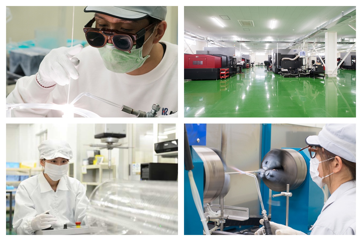
About Us
XKH specializes in high-tech development, production, and sales of special optical glass and new crystal materials. Our products serve optical electronics, consumer electronics, and the military. We offer Sapphire optical components, mobile phone lens covers, Ceramics, LT, Silicon Carbide SIC, Quartz, and semiconductor crystal wafers. With skilled expertise and cutting-edge equipment, we excel in non-standard product processing, aiming to be a leading optoelectronic materials high-tech enterprise.