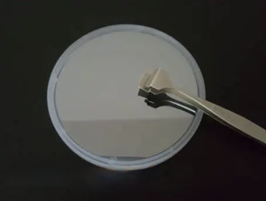
Silicon-On-Insulator Substrate SOI wafer three layers for Microelectronics and Radio Frequency
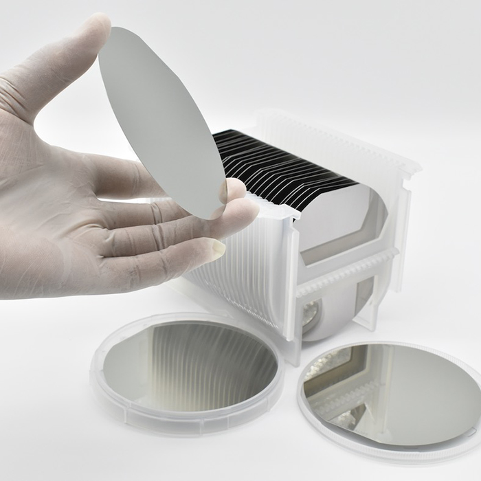

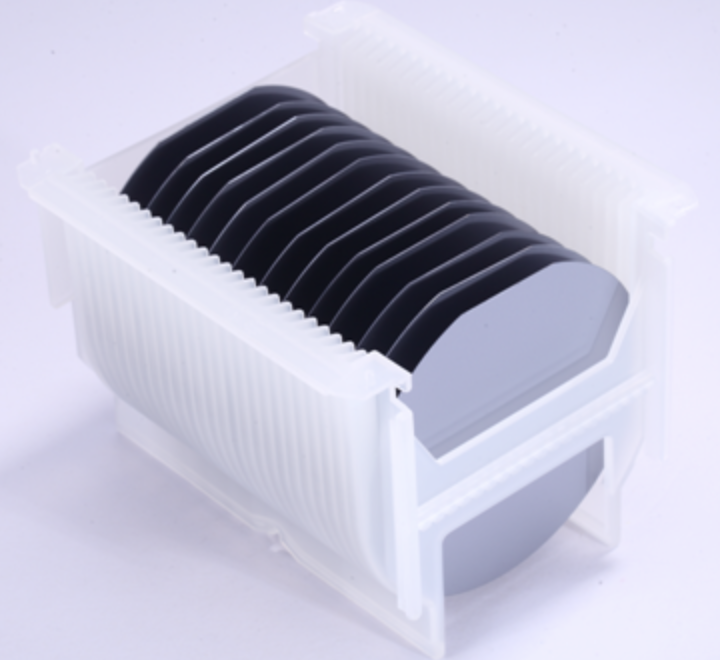
Introduce of wafer box
Introducing our advanced Silicon-On-Insulator (SOI) wafer, meticulously engineered with three distinct layers, revolutionizing microelectronics and radio frequency (RF) applications. This innovative substrate combines a top silicon layer, an insulating oxide layer, and a bottom silicon substrate to deliver unparalleled performance and versatility.
Designed for the demands of modern microelectronics, our SOI wafer provides a solid foundation for the fabrication of intricate integrated circuits (ICs) with superior speed, power efficiency, and reliability. The top silicon layer enables the seamless integration of complex electronic components, while the insulating oxide layer minimizes parasitic capacitance, enhancing overall device performance.
In the realm of RF applications, our SOI wafer excels with its low parasitic capacitance, high breakdown voltage, and excellent isolation properties. Ideal for RF switches, amplifiers, filters, and other RF components, this substrate ensures optimal performance in wireless communication systems, radar systems, and more.
Moreover, the inherent radiation tolerance of our SOI wafer makes it ideal for aerospace and defense applications, where reliability in harsh environments is critical. Its robust construction and exceptional performance characteristics guarantee consistent operation even in extreme conditions.
Key Features:
Three-Layer Architecture: Top silicon layer, insulating oxide layer, and bottom silicon substrate.
Superior Microelectronics Performance: Enables fabrication of advanced ICs with enhanced speed and power efficiency.
Excellent RF Performance: Low parasitic capacitance, high breakdown voltage, and superior isolation properties for RF devices.
Aerospace-Grade Reliability: Inherent radiation tolerance ensures reliability in harsh environments.
Versatile Applications: Suitable for a wide range of industries, including telecommunications, aerospace, defense, and more.
Experience the next generation of microelectronics and RF technology with our advanced Silicon-On-Insulator (SOI) wafer. Unlock new possibilities for innovation and drive progress in your applications with our cutting-edge substrate solution.
Detailed Diagram