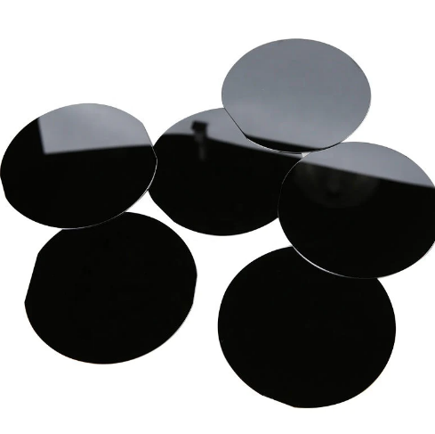
SOI wafer insulator on silicon 8-inch and 6-inch SOI (Silicon-On-Insulator) wafers


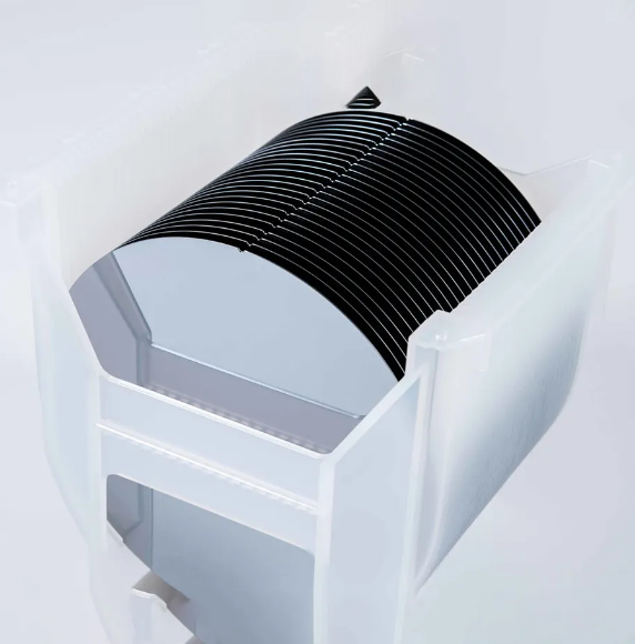
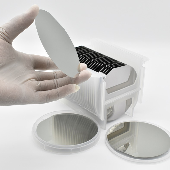
Introduce of wafer box
Comprising a top silicon layer, an insulating oxide layer, and a bottom silicon substrate, the three-layer SOI wafer offers unparalleled advantages in microelectronics and RF domains. The top silicon layer, featuring high-quality crystalline silicon, facilitates the integration of intricate electronic components with precision and efficiency. The insulating oxide layer, meticulously engineered to minimize parasitic capacitance, enhances device performance by mitigating unwanted electrical interference. The bottom silicon substrate provides mechanical support and ensures compatibility with existing silicon processing technologies.
In microelectronics, the SOI wafer serves as a foundation for the fabrication of advanced integrated circuits (ICs) with superior speed, power efficiency, and reliability. Its three-layer architecture enables the development of complex semiconductor devices such as CMOS (Complementary Metal-Oxide-Semiconductor) ICs, MEMS (Micro-Electro-Mechanical Systems), and power devices.
In the RF domain, the SOI wafer demonstrates remarkable performance in the design and implementation of RF devices and systems. Its low parasitic capacitance, high breakdown voltage, and excellent isolation properties make it an ideal substrate for RF switches, amplifiers, filters, and other RF components. Additionally, the SOI wafer's inherent radiation tolerance renders it suitable for aerospace and defense applications where reliability in harsh environments is paramount.
Furthermore, the versatility of the SOI wafer extends to emerging technologies such as photonic integrated circuits (PICs), where the integration of optical and electronic components on a single substrate holds promise for next-generation telecommunications and data communication systems.
In summary, the three-layer Silicon-On-Insulator (SOI) wafer stands at the forefront of innovation in microelectronics and RF applications. Its unique architecture and exceptional performance characteristics pave the way for advancements in diverse industries, driving progress and shaping the future of technology.
Detailed Diagram