SiC Dummy Wafer (EPI) CVD Process SiC epitaxy and MOCVD systems


Detailed Diagram


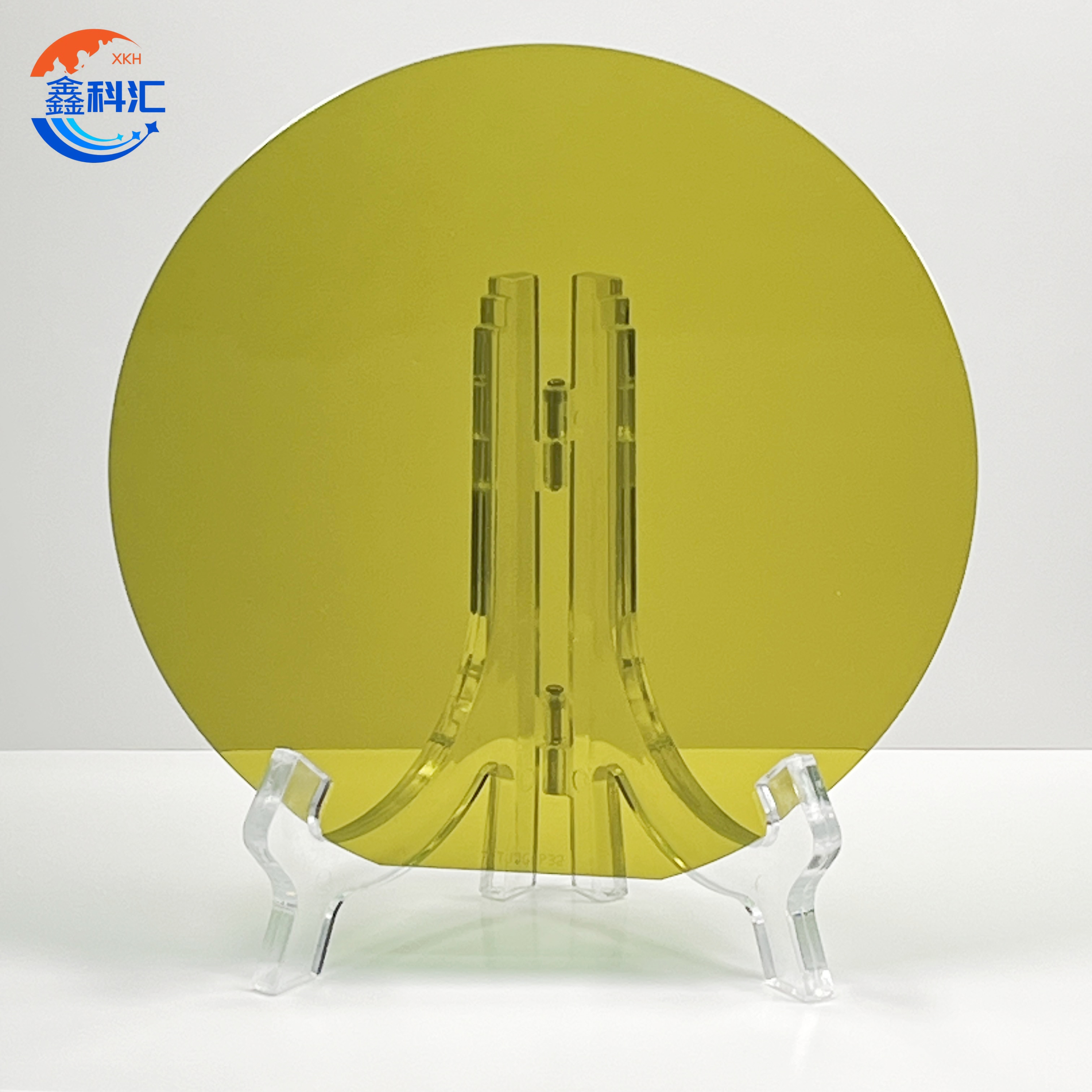
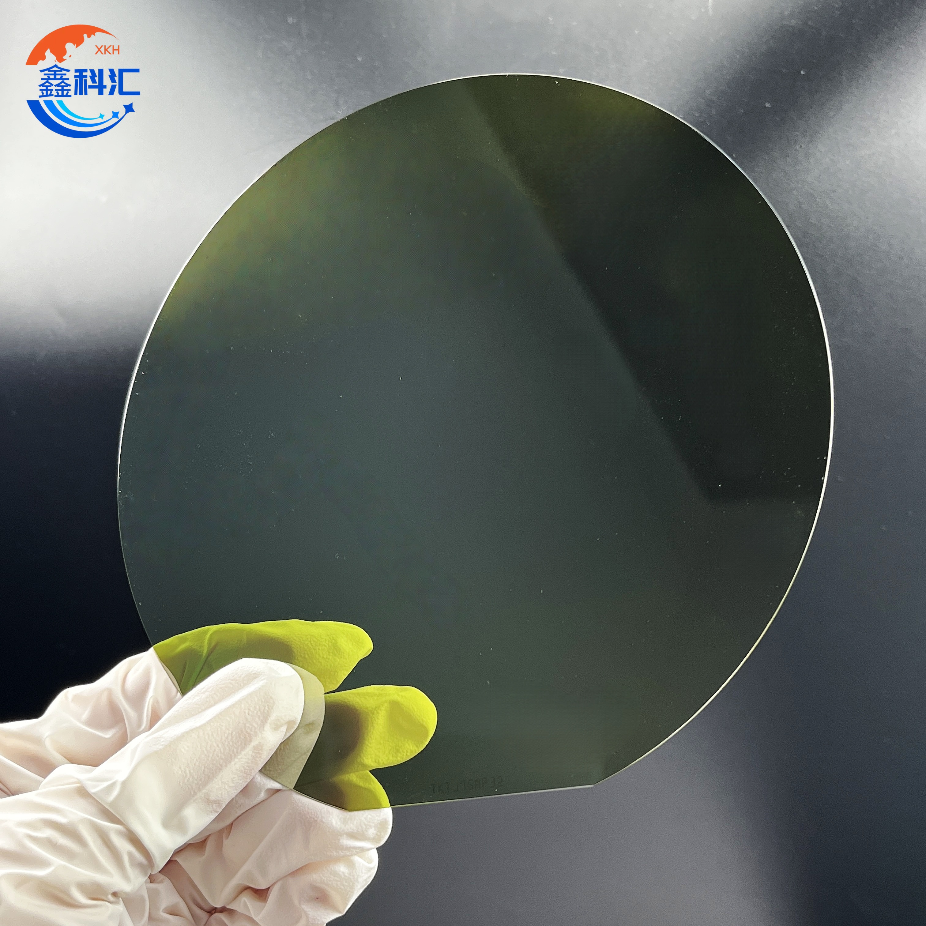
Overview of cvd sic epi wafer
SiC Epitaxial Wafers are now emerging as the most advanced form factor in the SiC industry. Representing the cutting edge of material science and manufacturing capability, 8” SiC epitaxial wafers offer unparalleled opportunities for scaling up power device production while driving down the cost per device.
As demand for electric vehicles, renewable energy, and industrial power electronics continues to surge globally, wafers are enabling a new generation of SiC MOSFETs, diodes, and integrated power modules with higher throughput, better yield, and lower manufacturing costs.
With wide bandgap properties, high thermal conductivity, and exceptional breakdown voltage, SiC wafers are unlocking new levels of performance and efficiency in advanced power electronics.
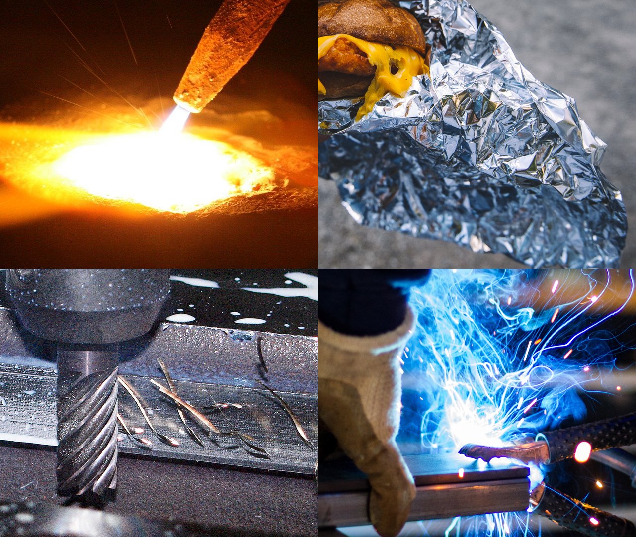
How SiC Epitaxial Wafers Are Made
Manufacturing SiC epitaxial wafers requires next-generation CVD reactors, precise crystal growth control, and ultra-flat substrate technology:
-
Substrate Fabrication
Monocrystalline SiC substrates are produced via high-temperature sublimation techniques and subsequently polished to sub-nanometer roughness. -
CVD Epitaxial Growth
Advanced large-scale CVD tools operate at ~1600 °C to deposit high-quality SiC epitaxial layers onto the 8” substrates, with optimized gas flow and temperature uniformity to handle the larger area. -
Tailored Doping
N-type or P-type doping profiles are created with high uniformity across the entire 300 mm wafer. -
Precision Metrology
Uniformity control, crystal defect monitoring, and in-situ process management ensure consistency from wafer center to edge. -
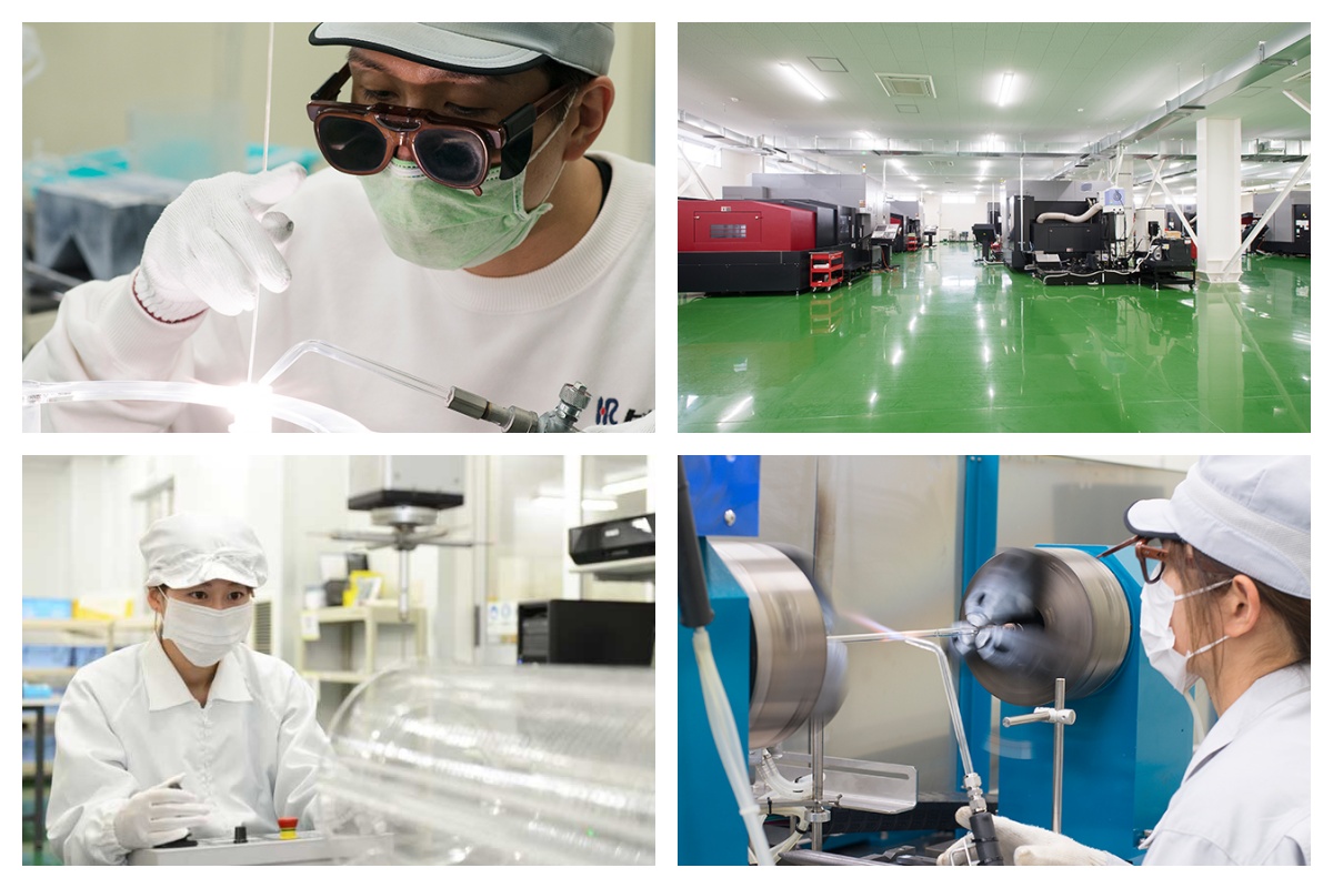
Comprehensive Quality Assurance
Each wafer is validated via:-
AFM, Raman, and XRD
-
Full-wafer defect mapping
-
Surface roughness and warp analysis
-
Electrical property measurements
-
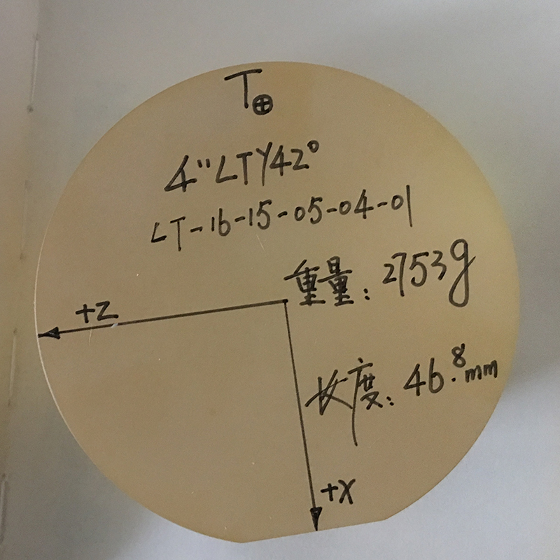
Specifications
| Grade | 8InchN-typeSiCSubstrate | ||
| 1 | Polytype | -- | 4HSiC |
| 2 | ConductivityType | -- | N |
| 3 | Diameter | mm | 200.00±0.5mm |
| 4 | Thickness | um | 700±50µm |
| 5 | CrystalSurfaceOrientationAxis | degree | 4.0°toward±0.5° |
| 6 | Notchdepth | mm | 1~1.25mm |
| 7 | Notchorientation | degree | ±5° |
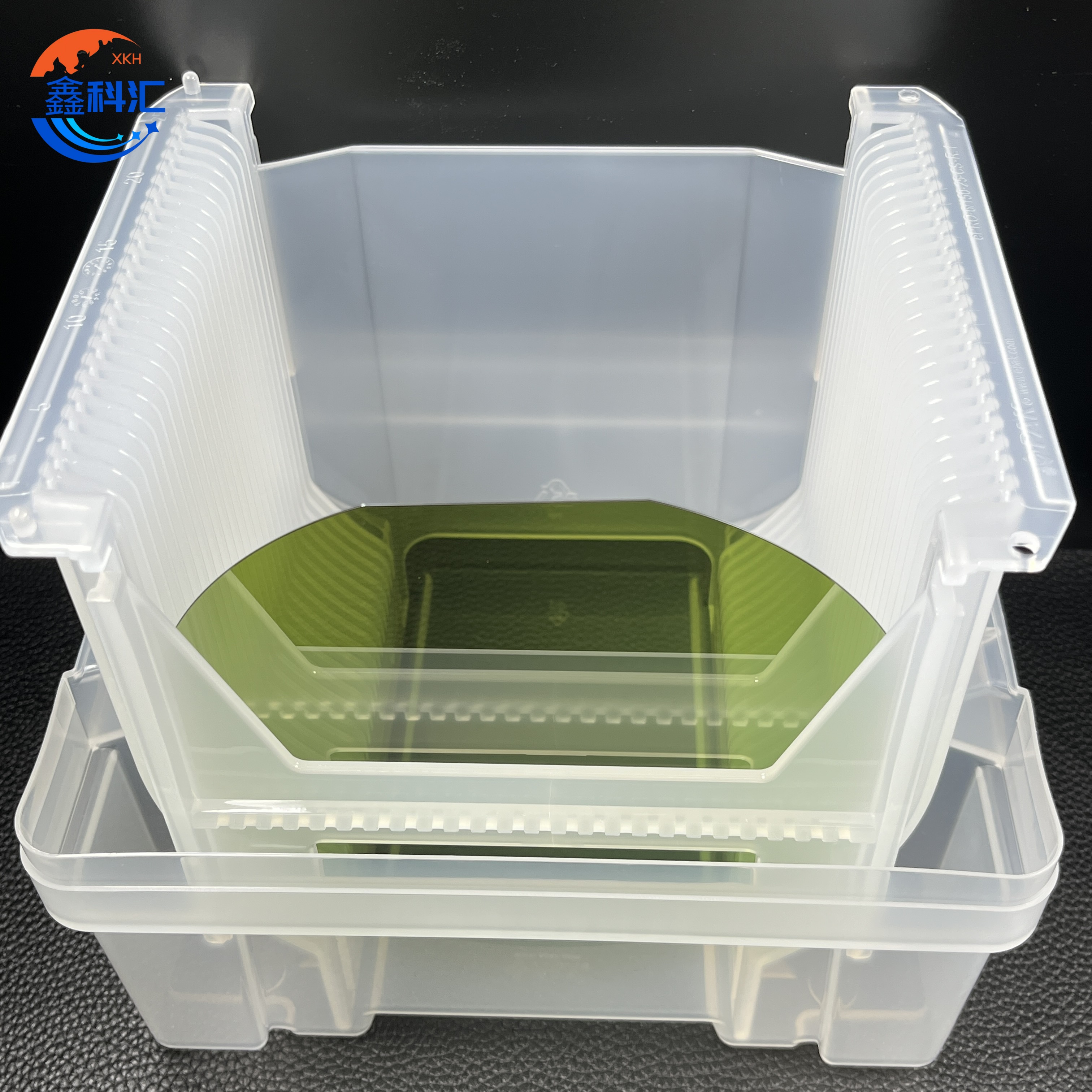
| 8 | Resistivity(Average) | Ωcm | NA |
| 9 | TTV | um | NA |
| 10 | LTV | um | NA |
| 11 | Bow | um | NA |
| 12 | Warp | um | NA |
| 13 | MPD | cm-2 | NA |
| 14 | TSD | cm-2 | NA |
| 15 | BPD | cm-2 | NA |
| 16 | TED | cm-2 | NA |
| 17 | EPD | cm-2 | NA |
| 18 | ForeignPolytypes | -- | NA |
| 19 | SF(BSF)(2x2mmgridsize) | % | NA |
| 20 | TUA(TotalUsableArea)(2x2mmgridsize) | % | NA |
| 21 | NominalEdgeExclusion | mm | NA |
| 22 | Visualscratches | -- | NA |
| 23 | Scratches-cumulativelength(SiSurface) | mm | NA |
| 24 | SiFace | -- | CMPpolished |
| 25 | CFace | -- | CMPpolished |
| 26 | Surfaceroughness(Siface) | nm | NA |
| 27 | Surfaceroughness(Cface) | nm | NA |
| 28 | lasermarking | -- | CFace,abovetheNotch |
| 29 | Edgechip(Front&backSurfaces) | -- | NA |
| 30 | Hexplates | -- | NA |
| 31 | Cracks | -- | NA |
| 32 | Particle(≥0.3um) | -- | NA |
| 33 | Areacontamination(stains) | -- | None:Bothfaces |
| 34 | ResidualMetalsContamination(ICP-MS) | atom/cm2 | NA |
| 35 | EdgeProfile | -- | Chamfer,R-Shape |
| 36 | Packaging | -- | Multi-waferCassetteOrSingleWaferContainer |
Applications
SiC epitaxial wafers enable mass production of reliable power devices in sectors including:
-
Electric Vehicles (EVs)
Traction inverters, onboard chargers, and DC/DC converters. -
Renewable Energy
Solar string inverters, wind power converters. -
Industrial Drives
Efficient motor drives, servo systems. -
5G / RF Infrastructure
Power amplifiers and RF switches. -
Consumer Electronics
Compact, high-efficiency power supplies.

Frequently Asked Questions (FAQ)
1. What is the benefit of SiC wafers?
They significantly reduce production cost per chip through increased wafer area and process yield.
2. How mature is SiC production?
8” is entering pilot production with select industry leaders—our wafers are available now for R&D and volume ramp.
3. Can doping and thickness be customized?
Yes, full customization of doping profile and epi thickness is available.
4. Are existing fabs compatible with SiC wafers?
Minor equipment upgrades are needed for full compatibility.
5. What is typical lead time?
6–10 weeks for initial orders; shorter for repeat volumes.
About Us
XKH specializes in high-tech development, production, and sales of special optical glass and new crystal materials. Our products serve optical electronics, consumer electronics, and the military. We offer Sapphire optical components, mobile phone lens covers, Ceramics, LT, Silicon Carbide SIC, Quartz, and semiconductor crystal wafers. With skilled expertise and cutting-edge equipment, we excel in non-standard product processing, aiming to be a leading optoelectronic materials high-tech enterprise.
Related Products
-

Customized SiC Seed Crystal Substrates Dia 205/...
-

sapphire ring made of synthetic sapphire materi...
-

Copper substrate Copper cubic Single crystal Cu...
-

SiCOI wafer 4inch 6inch HPSI SiC SiO2 Si subatr...
-
3inch 4 inch 6inch LiNbO3 Wafer Substrate Singl...
-
Step Holes Dia25.4×2.0mmt Sapphire optical...