LT Lithium Tantalate (LiTaO3) Crystal 2inch/3inch/4inch/6寸inch Orientaiton Y-42°/36°/108° Thickness 250-500um


Technical parameters
| Name | Optical-grade LiTaO3 | Sound table level LiTaO3 |
| Axial | Z cut + / - 0.2 ° | 36 ° Y cut / 42 ° Y cut / X cut(+ / - 0.2 °) |
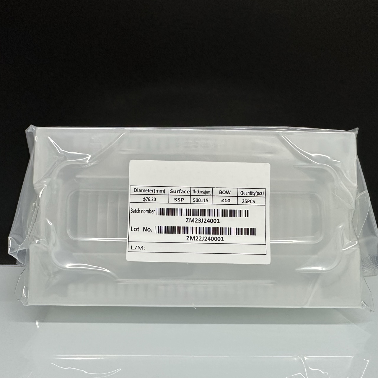
| Diameter | 76.2mm + / - 0.3mm/100±0.2mm | 76.2mm + /-0.3mm 100mm + /-0.3mm 0r 150±0.5mm |
| Datum plane | 22mm + / - 2mm | 22mm + /-2mm32mm + /-2mm |
| Thickness | 500um + /-5mm1000um + /-5mm | 500um + /-20mm350um + /-20mm |
| TTV | ≤ 10um | ≤ 10um |
| Curie temperature | 605 °C + / - 0.7 °C (DTAmethod) | 605 °C + / -3 °C (DTAmethod |
| Surface quality | Double-sided polishing | Double-sided polishing |
| Chamfered edges | edge rounding | edge rounding |
Key Characteristics
1.Crystal Structure and Electrical Performance
· Crystallographic Stability: 100% 4H-SiC polytype dominance, zero multicrystalline inclusions (e.g., 6H/15R), with XRD rocking curve full-width at half-maximum (FWHM) ≤32.7 arcsec.
· High Carrier Mobility: Electron mobility of 5,400 cm²/V·s (4H-SiC) and hole mobility of 380 cm²/V·s, enabling high-frequency device designs.
·Radiation Hardness: Withstands 1 MeV neutron irradiation with a displacement damage threshold of 1×10¹⁵ n/cm², ideal for aerospace and nuclear applications.
2.Thermal and Mechanical Properties
· Exceptional Thermal Conductivity: 4.9 W/cm·K (4H-SiC), triple that of silicon, supporting operation above 200°C.
· Low Thermal Expansion Coefficient: CTE of 4.0×10⁻⁶/K (25–1000°C), ensuring compatibility with silicon-based packaging and minimizing thermal stress.
3.Defect Control and Processing Precision
· Micropipe Density: <0.3 cm⁻² (8-inch wafers), dislocation density <1,000 cm⁻² (verified via KOH etching).
· Surface Quality: CMP-polished to Ra <0.2 nm, meeting EUV lithography-grade flatness requirements.
Key Applications
|
Domain |
Application Scenarios |
Technical Advantages |
|
Optical Communications |
100G/400G lasers, silicon photonics hybrid modules |
InP seed substrates enable direct bandgap (1.34 eV) and Si-based heteroepitaxy, reducing optical coupling loss. |
|
New Energy Vehicles |
800V high-voltage inverters, onboard chargers (OBC) |
4H-SiC substrates withstand >1,200 V, reducing conduction losses by 50% and system volume by 40%. |
|
5G Communications |
Millimeter-wave RF devices (PA/LNA), base station power amplifiers |
Semi-insulating SiC substrates (resistivity >10⁵ Ω·cm) enable high-frequency (60 GHz+) passive integration. |
|
Industrial Equipment |
High-temperature sensors, current transformers, nuclear reactor monitors |
InSb seed substrates (0.17 eV bandgap) deliver magnetic sensitivity up to 300%@10 T. |
LiTaO₃ Wafers - Key Characteristics
1. Superior Piezoelectric Performance
· High piezoelectric coefficients (d₃₃~8-10 pC/N, K²~0.5%) enable high-frequency SAW/BAW devices with insertion loss <1.5dB for 5G RF filters
· Excellent electromechanical coupling supports wide-bandwidth (≥5%) filter designs for sub-6GHz and mmWave applications
2. Optical Properties
· Broadband transparency (>70% transmission from 400-5000nm) for electro-optic modulators achieving >40GHz bandwidth
· Strong nonlinear optical susceptibility (χ⁽²⁾~30pm/V) facilitates efficient second harmonic generation (SHG) in laser systems
3. Environmental Stability
· High Curie temperature (600°C) maintains piezoelectric response in automotive-grade (-40°C to 150°C) environments
· Chemical inertness against acids/alkalies (pH1-13) ensures reliability in industrial sensor applications
4. Customization Capabilities
· Orientation engineering: X-cut (51°), Y-cut (0°), Z-cut (36°) for tailored piezoelectric responses
· Doping options: Mg-doped (optical damage resistance), Zn-doped (enhanced d₃₃)
· Surface finishes: Epitaxial-ready polishing (Ra<0.5nm), ITO/Au metallization
LiTaO₃ Wafers - Primary Applications
1. RF Front-End Modules
· 5G NR SAW filters (Band n77/n79) with temperature coefficient of frequency (TCF) <|-15ppm/°C|
· Ultra-wideband BAW resonators for WiFi 6E/7 (5.925-7.125GHz)
2. Integrated Photonics
· High-speed Mach-Zehnder modulators (>100Gbps) for coherent optical communications
· QWIP infrared detectors with cutoff wavelengths tunable from 3-14μm
3. Automotive Electronics
· Ultrasonic parking sensors with >200kHz operational frequency
· TPMS piezoelectric transducers surviving -40°C to 125°C thermal cycling
4. Defense Systems
· EW receiver filters with >60dB out-of-band rejection
· Missile seeker IR windows transmitting 3-5μm MWIR radiation
5. Emerging Technologies
· Optomechanical quantum transducers for microwave-to-optical conversion
· PMUT arrays for medical ultrasound imaging (>20MHz resolution)
LiTaO₃ Wafers - XKH Services
1. Supply Chain Management
· Boule-to-wafer processing with 4-week lead time for standard specifications
· Cost-optimized production delivering 10-15% price advantage versus competitors
2. Custom Solutions
· Orientation-specific wafering: 36°±0.5° Y-cut for optimal SAW performance
· Doped compositions: MgO (5mol%) doping for optical applications
Metallization services: Cr/Au (100/1000Å) electrode patterning
3. Technical Support
· Material characterization: XRD rocking curves (FWHM<0.01°), AFM surface analysis
· Device simulation: FEM modeling for SAW filter design optimization
Conclusion
LiTaO₃ wafers continue to enable technological advancements across RF communications, integrated photonics, and harsh-environment sensors. XKH's material expertise, manufacturing precision, and application engineering support help customers overcome design challenges in next-generation electronic systems.


Related Products
-

Laser Anti-Counterfeiting Marking System for Sa...
-

JGS1, JGS2, and JGS3 Fused Silica Optical Glass
-

Silicon Carbide Prism / Mirror For Infrared Opt...
-
3inch Dia76.2mm sapphire wafer 0.5mm thickness ...
-

4inch Silicon wafer FZ CZ N-Type DSP or SSP Tes...
-

SiC Epitaxial Wafer for Power Devices – 4H-SiC,...