LNOI Wafer (Lithium Niobate on Insulator) Telecommunications Sensing High Electro-Optic
Detailed Diagram


Overview
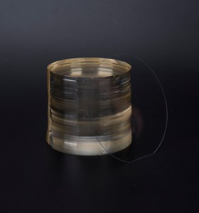
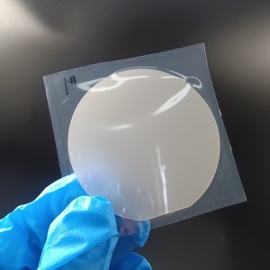
Inside the wafer box there are symmetrical grooves, the dimensions of which are strictly uniform to support the two sides of the wafer. The crystal box is generally made of translucent plastic PP material which is resistant to temperature, wear and static electricity. Different colors of additives are used to distinguish metal process segments in semiconductor production. Due to the small key size of semiconductors, dense patterns, and very strict particle size requirements in production, the wafer box must be guaranteed a clean environment to connect to the microenvironment box reaction cavity of different production machines.
Fabrication Methodology
The fabrication of LNOI wafers consists of several precise steps:
Step 1: Helium Ion Implantation Helium ions are introduced into a bulk LN crystal using an ion implanter. These ions lodge at a specific depth, forming a weakened plane that will eventually facilitate film detachment.
Step 2: Base Substrate Formation A separate silicon or LN wafer is oxidized or layered with SiO2 using PECVD or thermal oxidation. Its top surface is planarized for optimal bonding.
Step 3: Bonding of LN to Substrate The ion-implanted LN crystal is flipped and attached to the base wafer using direct wafer bonding. In research settings, benzocyclobutene (BCB) can be used as an adhesive to simplify bonding under less stringent conditions.
Step 4: Thermal Treatment and Film Separation Annealing activates bubble formation at the implanted depth, enabling separation of the thin film (top LN layer) from the bulk. Mechanical force is used to complete the exfoliation.
Step 5: Surface Polishing Chemical Mechanical Polishing (CMP) is applied to smooth the top LN surface, improving optical quality and device yield.
Technical Parameters
| Material |
Optical Grade LiNbO3 wafes(White or Black) |
|
| Curie Temp |
1142±0.7℃ |
|
| Cutting Angle |
X/Y/Z etc |
|
| Diameter/size |
2”/3”/4” ±0.03mm |
|
| Tol(±) |
<0.20 mm ±0.005mm |
|
| Thickness |
0.18~0.5mm or more |
|
| Primary Flat |
16mm/22mm/32mm |
|
| TTV |
<3μm |
|
| Bow |
-30<bow<30 |
|
| Warp |
<40μm |
|
| Orientation Flat |
All available |
|
| Surface Type |
Single Side Polished(SSP)/Double Sides Polished(DSP) |
|
| Polished side Ra |
<0.5nm |
|
| S/D |
20/10 |
|
| Edge Criteria | R=0.2mm C-type or Bullnose | |
| Quality | Free of crack(bubbles and inclusions) | |
| Optical doped | Mg/Fe/Zn/MgO etc for optical grade LN< wafers per requested | |
| Wafer Surface Criteria |
Refractive index |
No=2.2878/Ne=2.2033 @632nm wavelength/prism coupler method. |
|
Contamination, |
None | |
|
Particles c>0.3μ m |
<=30 | |
|
Scratch,Chipping |
None | |
|
Defect |
No edge cracks,scratches,saw marks,stains | |
| Packaging |
Qty/Wafer box |
25pcs per box |
Use Cases
Due to its versatility and performance, LNOI is used across numerous industries:
Photonics: Compact modulators, multiplexers, and photonic circuits.
RF/Acoustics: Acousto-optic modulators, RF filters.
Quantum Computing: Nonlinear frequency mixers and photon-pair generators.
Defense & Aerospace: Low-loss optical gyros, frequency-shifting devices.
Medical Devices: Optical biosensors and high-frequency signal probes.
FAQ
Q: Why is LNOI preferred over SOI in optical systems?
A: LNOI features superior electro-optic coefficients and wider transparency range, enabling higher performance in photonic circuits.
Q: Is CMP mandatory after splitting?
A: Yes. The exposed LN surface is rough after ion-slicing and must be polished to meet optical-grade specifications.
Q: What is the maximum wafer size available?
A: Commercial LNOI wafers are primarily 3” and 4”, though some suppliers are developing 6” variants.
Q: Can the LN layer be re-used post-splitting?
A: The base crystal can be re-polished and reused several times, although the quality may degrade after multiple cycles.
Q: Are LNOI wafers compatible with CMOS processing?
A: Yes, they are designed to align with conventional semiconductor fabrication processes, especially when silicon substrates are used.


