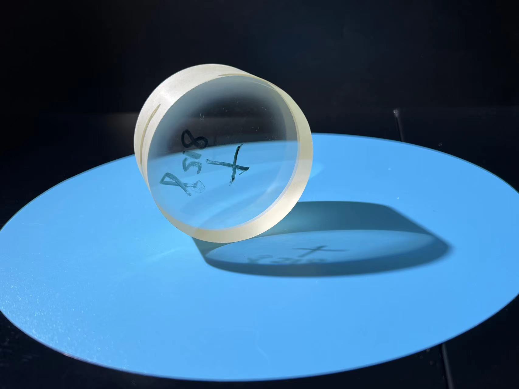
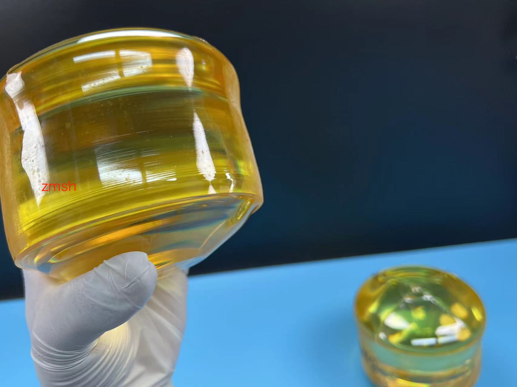
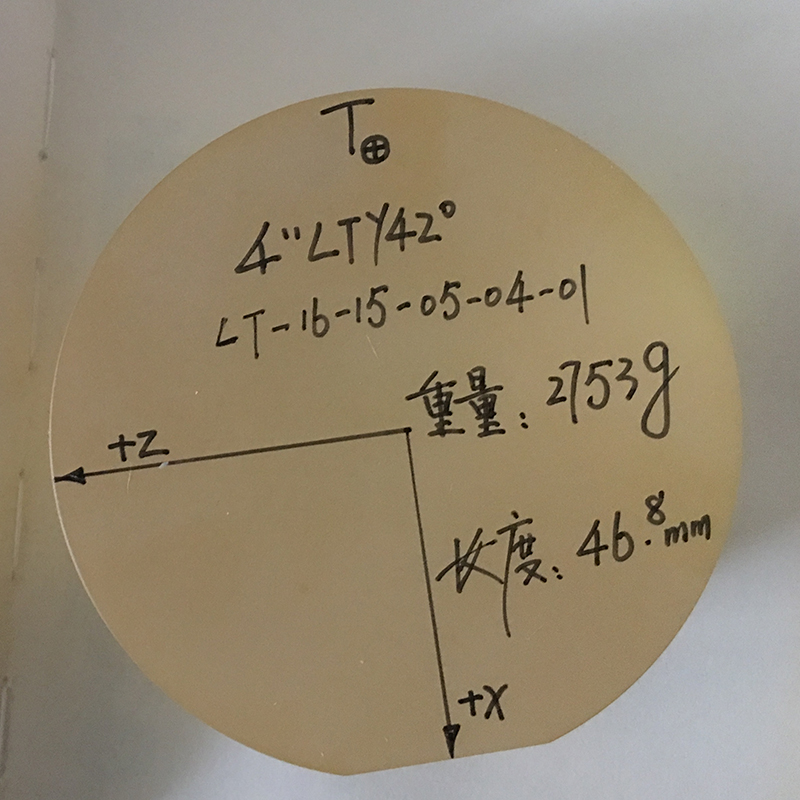
8 Inch Lithium Niobate Wafer LiNbO3 LN wafer


Detailed Information
| Diameter | 200±0.2mm |
| major flatness | 57.5mm, Notch |
| Orientation | 128Y-Cut, X-Cut, Z-Cut |
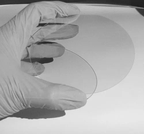
| Thickness | 0.5±0.025mm, 1.0±0.025mm |
| Surface | DSP and SSP |
| TTV | < 5µm |
| BOW | ± (20µm ~40um ) |
| Warp | <= 20µm ~ 50µm |
| LTV (5mmx5mm) | <1.5 um |
| PLTV(<0.5um) | ≥98% (5mm*5mm) with 2mm edge excluded |
| Ra | Ra<=5A |
| Scratch & Dig (S/D) | 20/10, 40/20, 60/40 |
| Edge | Meet SEMI M1.2@with GC800#. regular at C type |
Specific specifications
Diameter :8 inches (approximately 200mm)
Thickness: Common standard thicknesses range from 0.5mm to 1mm. Other thicknesses can be customized according to specific requirements
Crystal orientation: The main common crystal orientation is 128Y-cut,Z-cut and X-cut crystal orientation, and other crystal orientation can be provided depending on the specific application
Size Advantages: 8-inch serrata carp wafers have several size advantages over smaller wafers:
Larger area: Compared to 6-inch or 4-inch wafers, 8-inch wafers provide a larger surface area and can accommodate more devices and integrated circuits, resulting in increased production efficiency and yield.
Higher density: By using 8-inch wafers, more devices and components can be realized in the same area, increasing integration and device density, which in turn enhances device performance.
Better consistency: Larger wafers have better consistency in the production process, helping to reduce variability in the manufacturing process and improve product reliability and consistency.
The 8-inch L and LN wafers have the same diameter as mainstream silicon wafers and are easy to bond. As a high performance "jointed SAW filter" material that can handle high frequency bands.
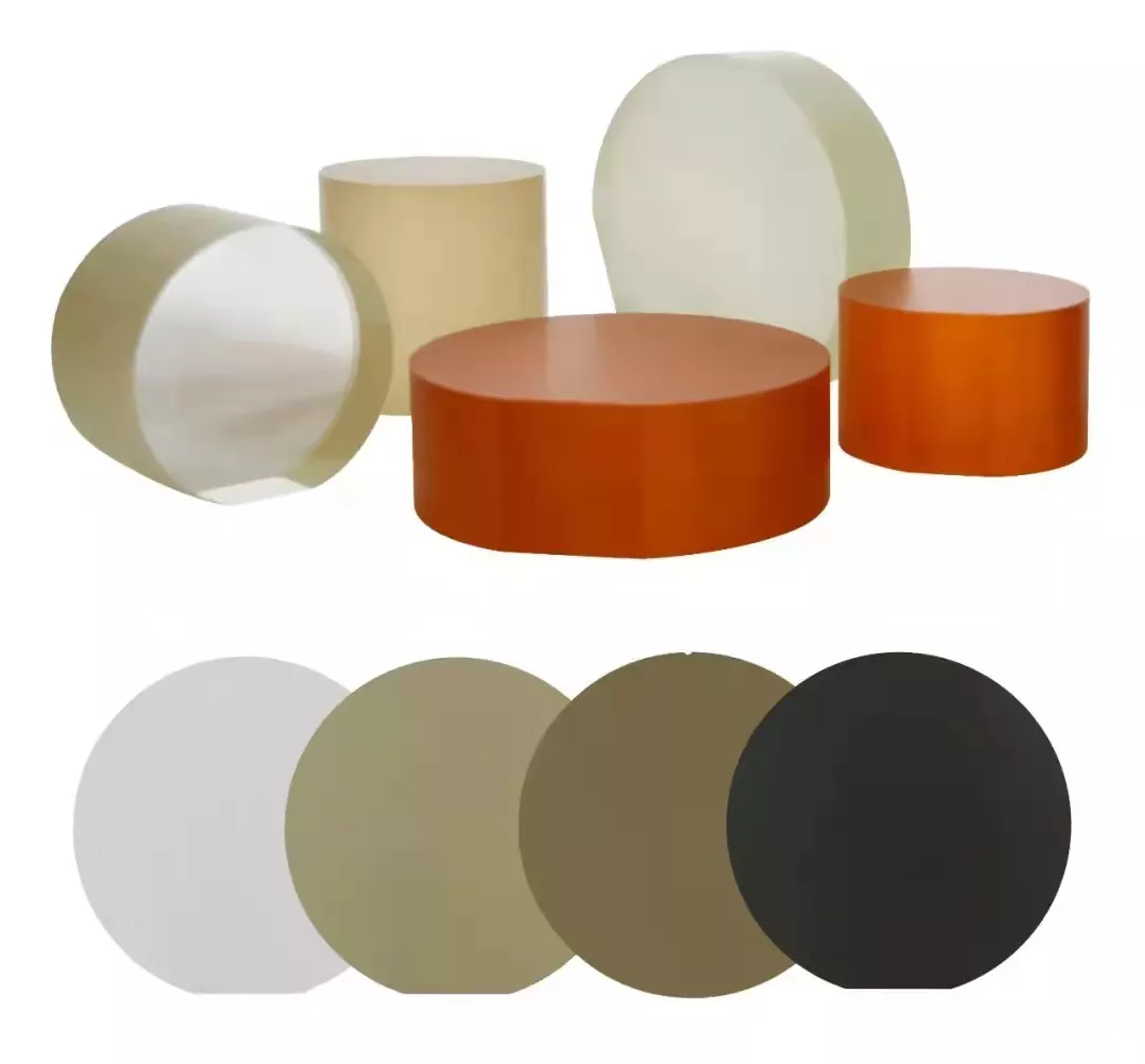
Detailed Diagram