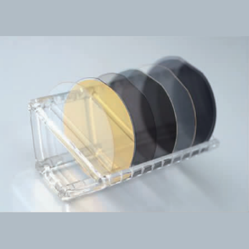
8inch LNOI (LiNbO3 on Insulator) Wafer for Optical Modulators Waveguides Integrated Circuits


Detailed Diagram
Introduction
Lithium Niobate on Insulator (LNOI) wafers are a cutting-edge material used in various advanced optical and electronic applications. These wafers are produced by transferring a thin layer of lithium niobate (LiNbO₃) onto an insulating substrate, typically silicon or another suitable material, using sophisticated techniques like ion implantation and wafer bonding. LNOI technology shares many similarities with Silicon on Insulator (SOI) wafer technology but takes advantage of the unique optical properties of lithium niobate, a material known for its piezoelectric, pyroelectric, and nonlinear optical characteristics.
LNOI wafers have gained significant attention in fields such as integrated optics, telecommunications, and quantum computing due to their superior performance in high-frequency and high-speed applications. The wafers are produced using the "Smart-cut" technique, which enables precise control over the thickness of the lithium niobate thin film, ensuring the wafers meet the required specifications for various applications.
Principle
The process of creating LNOI wafers begins with a bulk lithium niobate crystal. The crystal undergoes ion implantation, where high-energy helium ions are introduced into the surface of the lithium niobate crystal. These ions penetrate the crystal to a specific depth and disrupt the crystal structure, creating a fragile plane that can later be used to separate the crystal into thin layers. The specific energy of the helium ions controls the depth of implantation, which directly impacts the thickness of the final lithium niobate layer.
After ion implantation, the lithium niobate crystal is bonded to a substrate using a technique called wafer bonding. The bonding process typically uses a direct bonding method, where the two surfaces (the ion-implanted lithium niobate crystal and the substrate) are pressed together under high temperature and pressure to create a strong bond. In some cases, an adhesive material like benzocyclobutene (BCB) may be used for additional support.
Following bonding, the wafer undergoes an annealing process to repair any damage caused by the ion implantation and to enhance the bond between the layers. The annealing process also helps the thin lithium niobate layer to detach from the original crystal, leaving behind a thin, high-quality layer of lithium niobate that can be used for device fabrication.
Specifications
LNOI wafers are characterized by several important specifications that ensure their suitability for high-performance applications. These include:
Material Specifications
|
Material |
Specifications |
|
Material |
Homogeneous: LiNbO3 |
|
Material Quality |
Bubbles or inclusions <100μm<br>Quantity <8, 30μm < bubble size <100μm |
|
Orientation |
Y-cut ±0.2° |
|
Density |
4.65 g/cm³ |
|
Curie Temperature |
1142 ±1°C |
|
Transparency |
>95% in 450-700 nm range (10 mm thickness) |
Manufacturing Specifications
|
Parameter |
Specification |
|
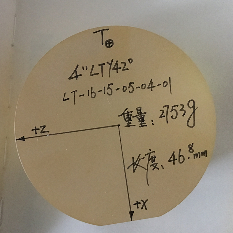
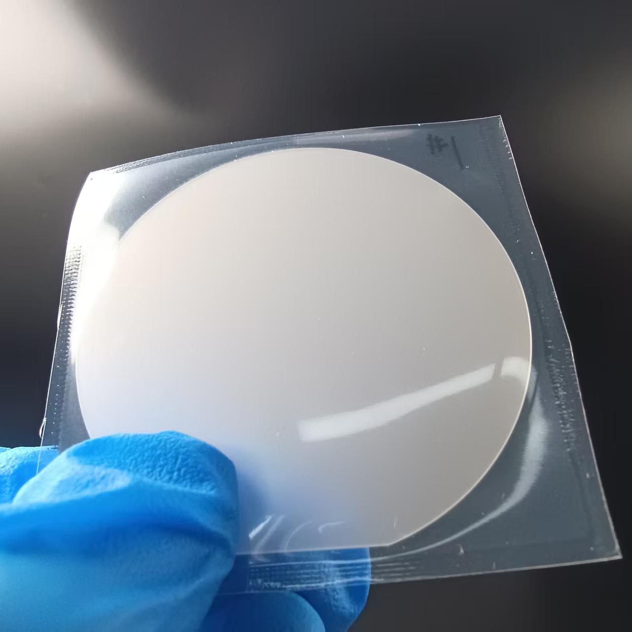
Diameter |
150 mm ±0.2 mm |
|
Thickness |
350 μm ±10 μm |
|
Flatness |
<1.3 μm |
|
Total Thickness Variation (TTV) |
Warp <70 μm @ 150 mm wafer |
|
Local Thickness Variation (LTV) |
<70 μm @ 150 mm wafer |
|
Roughness |
Rq ≤0.5 nm (AFM RMS value) |
|
Surface Quality |
40-20 |
|
Particles (Non-removable) |
100-200 μm ≤3 particles<br>20-100 μm ≤20 particles |
|
Chips |
<300 μm (full wafer, no exclusion zone) |
|
Cracks |
No cracks (full wafer) |
|
Contamination |
No non-removable stains (full wafer) |
|
Parallelism |
<30 arcseconds |
|
Orientation Reference Plane (X-axis) |
47 ±2 mm |
Applications
LNOI wafers are used in a wide range of applications due to their unique properties, particularly in the fields of photonics, telecommunications, and quantum technologies. Some of the key applications include:
Integrated Optics: LNOI wafers are widely used in integrated optical circuits, where they enable high-performance photonic devices such as modulators, waveguides, and resonators. The high nonlinear optical properties of lithium niobate make it an excellent choice for applications requiring efficient light manipulation.
Telecommunications: LNOI wafers are used in optical modulators, which are essential components in high-speed communication systems, including fiber optic networks. The ability to modulate light at high frequencies makes LNOI wafers ideal for modern telecommunication systems.
Quantum Computing: In quantum technologies, LNOI wafers are used to fabricate components for quantum computers and quantum communication systems. The nonlinear optical properties of LNOI are leveraged to create entangled photon pairs, which are critical for quantum key distribution and quantum cryptography.
Sensors: LNOI wafers are used in various sensing applications, including optical and acoustic sensors. Their ability to interact with both light and sound makes them versatile for different types of sensing technologies.
FAQ
Q:What is LNOI technology?
A:LNOI technology involves the transfer of a thin lithium niobate film onto an insulating substrate, typically silicon. This technology leverages the unique properties of lithium niobate, such as its high nonlinear optical characteristics, piezoelectricity, and pyroelectricity, making it ideal for integrated optics and telecommunications.
Q:What is the difference between LNOI and SOI wafers?
A:Both LNOI and SOI wafers are similar in that they consist of a thin layer of material bonded to a substrate. However, LNOI wafers use lithium niobate as the thin film material, while SOI wafers use silicon. The key difference lies in the properties of the thin film material, with LNOI offering superior optical and piezoelectric properties.
Q:What are the advantages of using LNOI wafers?
A:The main advantages of LNOI wafers include their excellent optical properties, such as high nonlinear optical coefficients, and their mechanical strength. These characteristics make LNOI wafers ideal for use in high-speed, high-frequency, and quantum applications.
Q:Can LNOI wafers be used for quantum applications?
A:Yes, LNOI wafers are widely used in quantum technologies due to their ability to generate entangled photon pairs and their compatibility with integrated photonics. These properties are crucial for applications in quantum computing, communication, and cryptography.
Q:What is the typical thickness of LNOI films?
A:LNOI films typically range from a few hundred nanometers to several micrometers in thickness, depending on the specific application. The thickness is controlled during the ion implantation process.