HPSI SiC Wafer ≥90% Transmittance Optical Grade for AI/AR Glasses


Core Introduction: The Role of HPSI SiC Wafers in AI/AR Glasses
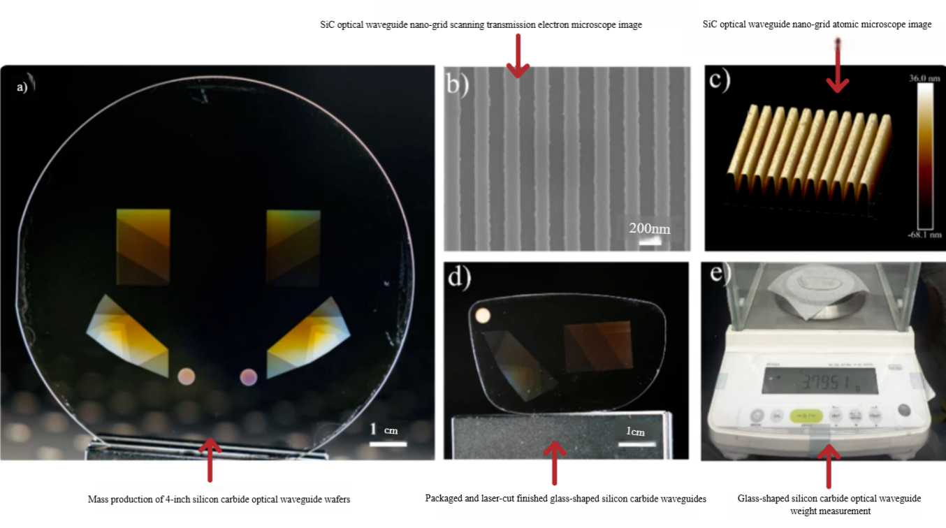
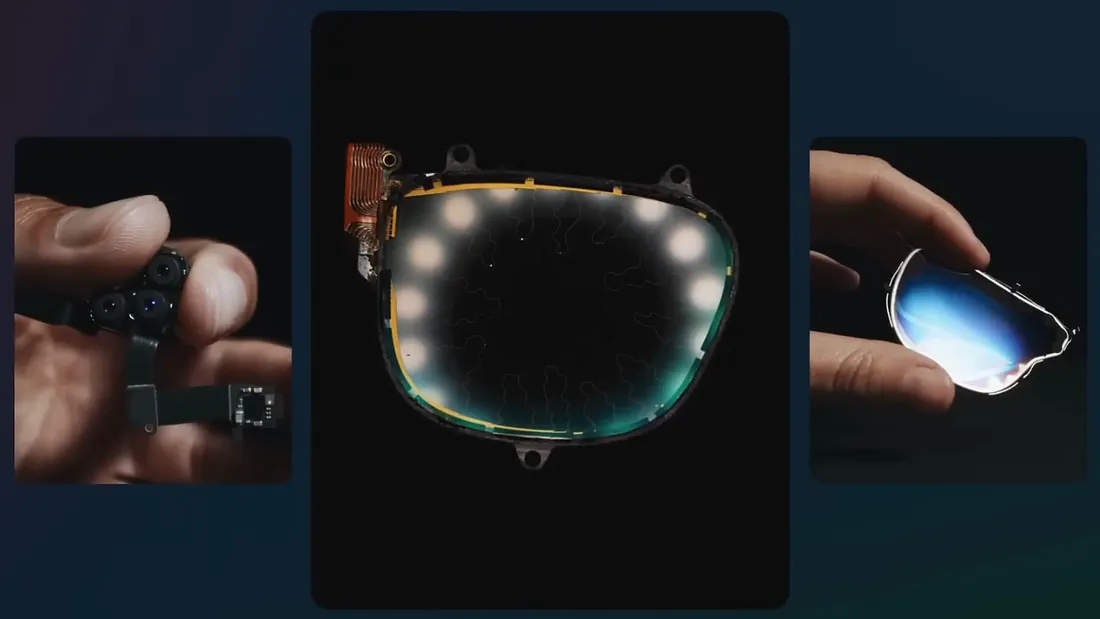
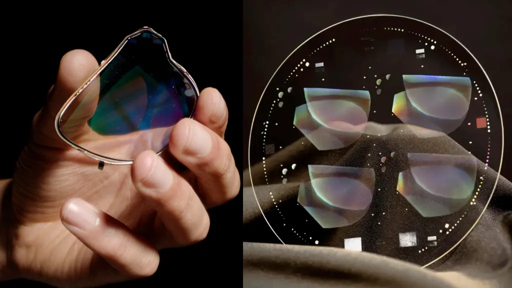
HPSI (High-Purity Semi-Insulating) Silicon Carbide wafers are specialized wafers characterized by high resistivity (>10⁹ Ω·cm) and extremely low defect density. In AI/AR glasses, they primarily serve as the core substrate material for diffractive optical waveguide lenses, addressing bottlenecks associated with traditional optical materials in terms of thin-and-light form factors, heat dissipation, and optical performance. For instance, AR glasses utilizing SiC waveguide lenses can achieve an ultra-wide field of view (FOV) of 70°–80°, while reducing the thickness of a single lens layer to just 0.55mm and weight to merely 2.7g, significantly enhancing wearing comfort and visual immersion.
Key Characteristics: How SiC Material Empowers AI/AR Glasses Design
High Refractive Index and Optical Performance Optimization
- SiC's refractive index (2.6–2.7) is nearly 50% higher than that of traditional glass (1.8–2.0). This allows for thinner and more efficient waveguide structures, significantly expanding the FOV. The high refractive index also helps suppress the "rainbow effect" common in diffractive waveguides, improving image purity.
Exceptional Thermal Management Capability
- With a thermal conductivity as high as 490 W/m·K (close to that of copper), SiC can rapidly dissipate heat generated by Micro-LED display modules. This prevents performance degradation or device aging due to high temperatures, ensuring long battery life and high stability.
Mechanical Strength and Durability
- SiC has a Mohs hardness of 9.5 (second only to diamond), offering exceptional scratch resistance, making it ideal for frequently used consumer glasses. Its surface roughness can be controlled to Ra < 0.5 nm, ensuring low-loss and highly uniform light transmission in waveguides.
Electrical Property Compatibility
- HPSI SiC's resistivity (>10⁹ Ω·cm) helps prevent signal interference. It can also serve as an efficient power device material, optimizing the power management modules in AR glasses.
Primary Application Directions
Core Optical Components for AI/AR Glasses
- Diffractive Waveguide Lenses: SiC substrates are used to create ultra-thin optical waveguides supporting large FOV and elimination of the rainbow effect.
- Window Plates and Prisms:Through customized cutting and polishing, SiC can be processed into protective windows or optical prisms for AR glasses, enhancing light transmittance and wear resistance.
Extended Applications in Other Fields
- Power Electronics: Used in high-frequency, high-power scenarios like new energy vehicle inverters and industrial motor controls.
- Quantum Optics: Acts as a host for color centers, used in substrates for quantum communication and sensing devices.
4 Inch & 6 Inch HPSI SiC Substrate Specification Comparison
|
Parameter |
Grade |
4-Inch Substrate |
6-Inch Substrate |
|
Diameter |
Z Grade / D Grade |
99.5 mm - 100.0 mm |
149.5 mm - 150.0 mm |
|
Poly-type |
Z Grade / D Grade |
4H |
4H |
|
Thickness |
Z Grade |
500 μm ± 15 μm |
500 μm ± 15 μm |
|
D Grade |
500 μm ± 25 μm |
500 μm ± 25 μm |
|
|
Wafer Orientation |
Z Grade / D Grade |
On axis: <0001> ± 0.5° |
On axis: <0001> ± 0.5° |
|
Micropipe Density |
Z Grade |
≤ 1 cm² |
≤ 1 cm² |
|
D Grade |
≤ 15 cm² |
≤ 15 cm² |
|
|
Resistivity |
Z Grade |
≥ 1E10 Ω·cm |
≥ 1E10 Ω·cm |
|
D Grade |
≥ 1E5 Ω·cm |
≥ 1E5 Ω·cm |
|
|
Primary Flat Orientation |
Z Grade / D Grade |
(10-10) ± 5.0° |
(10-10) ± 5.0° |
|
Primary Flat Length |
Z Grade / D Grade |
32.5 mm ± 2.0 mm |
Notch |
|
Secondary Flat Length |
Z Grade / D Grade |
18.0 mm ± 2.0 mm |
- |
|
Edge Exclusion |
Z Grade / D Grade |
3 mm |
3 mm |
|
LTV / TTV / Bow / Warp |
Z Grade |
≤ 2.5 μm / ≤ 5 μm / ≤ 15 μm / ≤ 30 μm |
≤ 2.5 μm / ≤ 6 μm / ≤ 25 μm / ≤ 35 μm |
|
D Grade |
≤ 10 μm / ≤ 15 μm / ≤ 25 μm / ≤ 40 μm |
≤ 5 μm / ≤ 15 μm / ≤ 40 μm / ≤ 80 μm |
|
|
Roughness |
Z Grade |
Polish Ra ≤ 1 nm / CMP Ra ≤ 0.2 nm |
Polish Ra ≤ 1 nm / CMP Ra ≤ 0.2 nm |
|
D Grade |
Polish Ra ≤ 1 nm / CMP Ra ≤ 0.2 nm |
Polish Ra ≤ 1 nm / CMP Ra ≤ 0.5 nm |
|
|
Edge Cracks |
D Grade |
Cumulative area ≤ 0.1% |
Cumulative length ≤ 20 mm, single ≤ 2 mm |
|
Polytype Areas |
D Grade |
Cumulative area ≤ 0.3% |
Cumulative area ≤ 3% |
|
Visual Carbon Inclusions |
Z Grade |
Cumulative area ≤ 0.05% |
Cumulative area ≤ 0.05% |
|
D Grade |
Cumulative area ≤ 0.3% |
Cumulative area ≤ 3% |
|
|
Silicon Surface Scratches |
D Grade |
5 allowed, each ≤1mm |
Cumulative length ≤ 1 x diameter |
|
Edge Chips |
Z Grade |
None permitted (width and depth ≥0.2mm) |
None permitted (width and depth ≥0.2mm) |
|
D Grade |
7 allowed, each ≤1mm |
7 allowed, each ≤1mm |
|
|
Threading Screw Dislocation |
Z Grade |
- |
≤ 500 cm² |
|
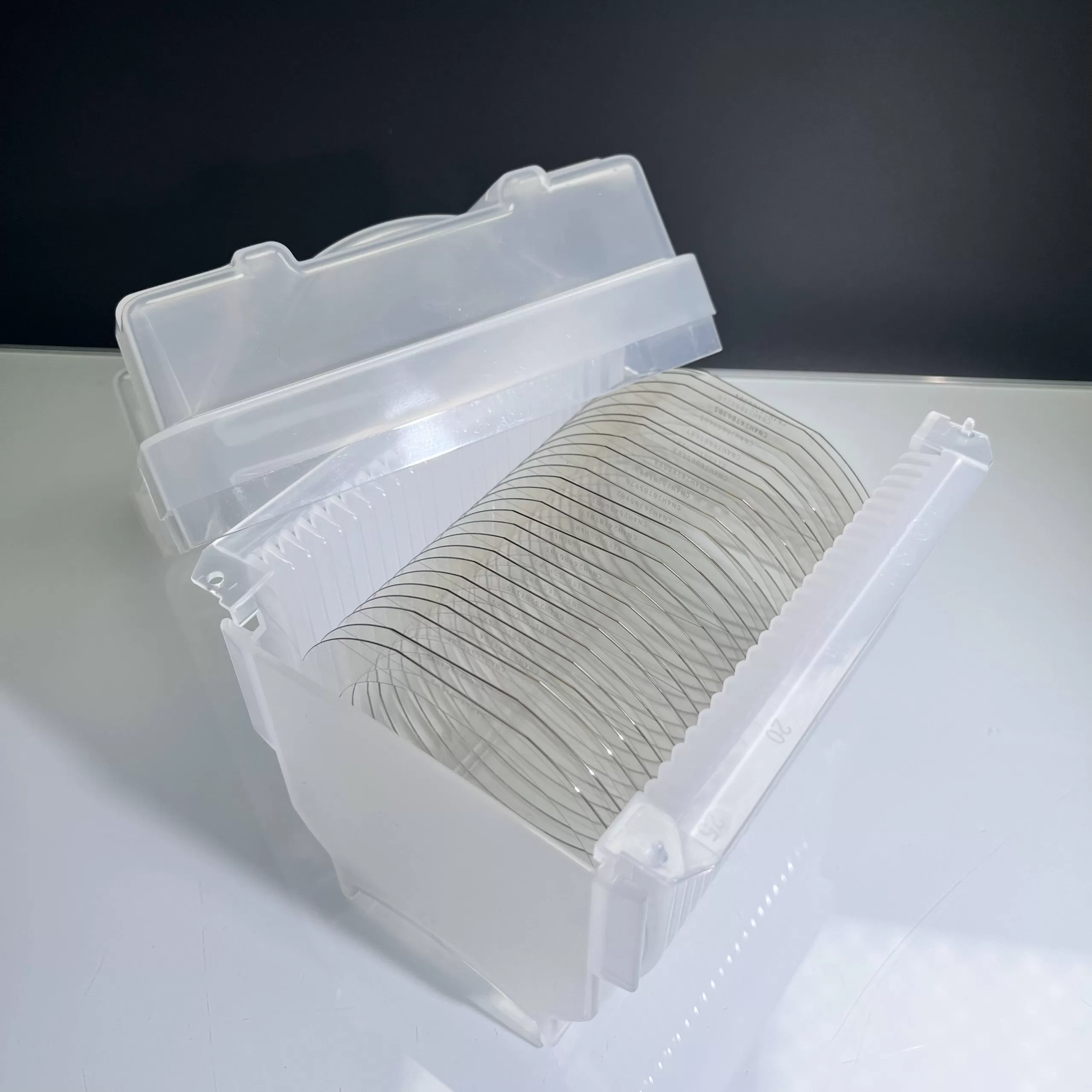
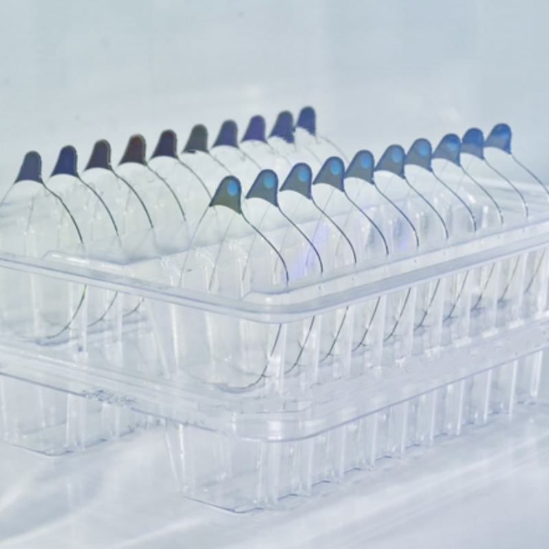
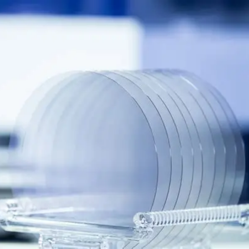
Packaging |
Z Grade / D Grade |
Multi-wafer Cassette Or Single Wafer Container |
Multi-wafer Cassette Or Single Wafer Container |
XKH Services: Integrated Manufacturing and Customization Capabilities
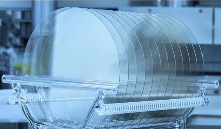
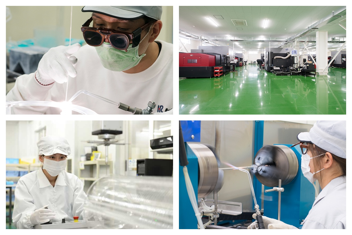
XKH company possesses vertical integration capabilities from raw materials to finished wafers, covering the entire chain of SiC substrate growth, slicing, polishing, and custom processing. Key service advantages include:
- Material Diversity: We can provide various wafer types like 4H-N type, 4H-HPSI type, 4H/6H-P type, and 3C-N type. Resistivity, thickness, and orientation can be adjusted according to requirements.
- Flexible Size Customization: We support wafer processing from 2-inch to 12-inch diameters, and can also process special structures like square pieces (e.g., 5x5mm, 10x10mm) and irregular prisms.
- Optical-Grade Precision Control: Wafer Total Thickness Variation (TTV) can be maintained at <1μm, and surface roughness at Ra < 0.3 nm, meeting the nano-level flatness requirements for waveguide devices.
- Rapid Market Response: The integrated business model ensures efficient transition from R&D to mass production, supporting everything from small-batch verification to large-volume shipments (lead time typically 15-40 days).
FAQ of HPSI SiC Wafer
Q1: Why is HPSI SiC considered an ideal material for AR waveguide lenses?
A1: Its high refractive index (2.6–2.7) enables thinner, more efficient waveguide structures that support a larger field of view (e.g., 70°–80°) while eliminating the "rainbow effect".
Q2: How does HPSI SiC improve thermal management in AI/AR glasses?
A2: With a thermal conductivity up to 490 W/m·K (close to copper), it efficiently dissipates heat from components like Micro-LEDs, ensuring stable performance and longer device lifespan.
Q3: What durability advantages does HPSI SiC offer for wearable glasses?
A3: Its exceptional hardness (Mohs 9.5) provides superior scratch resistance, making it highly durable for daily use in consumer-grade AR glasses.
Related Products
-

SiC Ingot 4H type Dia 4inch 6inch Thickness 5-1...
-

6inch 150mm Silicon Carbide SiC Wafers 4H-N typ...
-

P-type SiC substrate SiC wafer Dia2inch new pro...
-

N-Type SiC on Si Composite Substrates Dia6inch
-

SiC Epitaxial Wafer for Power Devices – 4H-SiC,...
-

4H-N/6H-N SiC Wafer Reasearch production Dummy ...