3inch Dia76.2mm SiC substrates HPSI Prime Research and Dummy grade


Silicon carbide substrates can be divided into two categories
Conductive substrate: refers to the resistivity of 15~30mΩ-cm silicon carbide substrate. The silicon carbide epitaxial wafer grown from the conductive silicon carbide substrate can be further made into power devices, which are widely used in new energy vehicles, photovoltaics, smart grids, and rail transport.
Semi-insulating substrate refers to the resistivity higher than 100000Ω-cm silicon carbide substrate, mainly used in the manufacture of gallium nitride microwave radio frequency devices, is the basis of wireless communication field.
It is a basic component in the field of wireless communication.
Silicon carbide conductive and semi-insulating substrates are used in a wide range of electronic devices and power devices, including but not limited to the following:
High-power semiconductor devices (conductive): Silicon carbide substrates have high breakdown field strength and thermal conductivity, and are suitable for the production of high-power power transistors and diodes and other devices.
RF electronic devices (semi-insulated): Silicon Carbide substrates have high switching speed and power tolerance, suitable for applications such as RF power amplifiers, microwave devices and high frequency switches.
Optoelectronic devices (semi-insulated): Silicon carbide substrates have a wide energy gap and high thermal stability, suitable for making photodiodes, solar cells and laser diodes and other devices.
Temperature sensors (conductive): Silicon carbide substrates have high thermal conductivity and thermal stability, suitable for the production of high-temperature sensors and temperature measurement instruments.
The production process and application of silicon carbide conductive and semi-insulating substrates have a wide range of fields and potentials, providing new possibilities for the development of electronic devices and power devices.
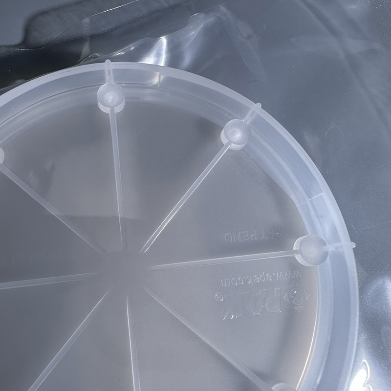
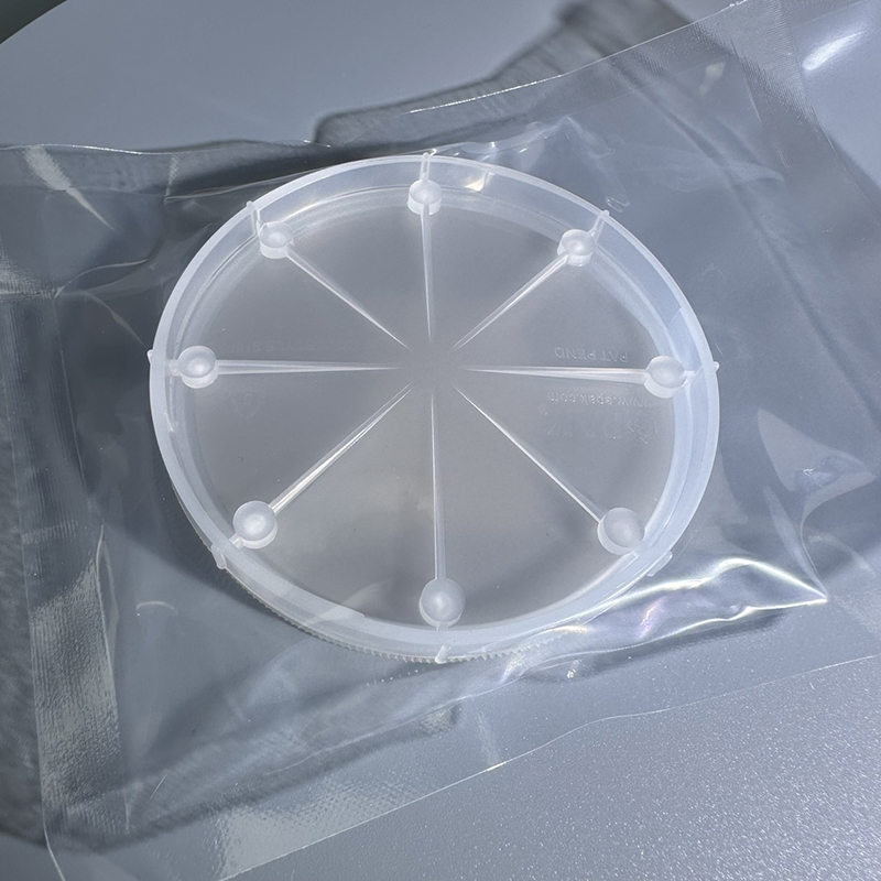
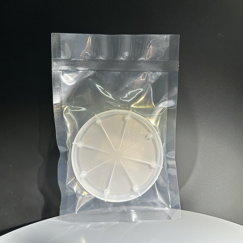
Detailed Diagram