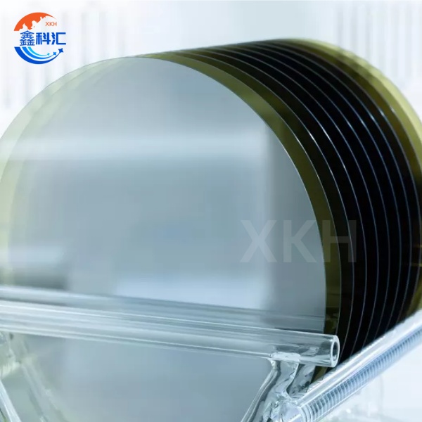
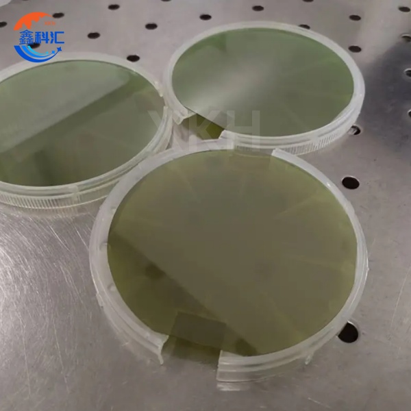
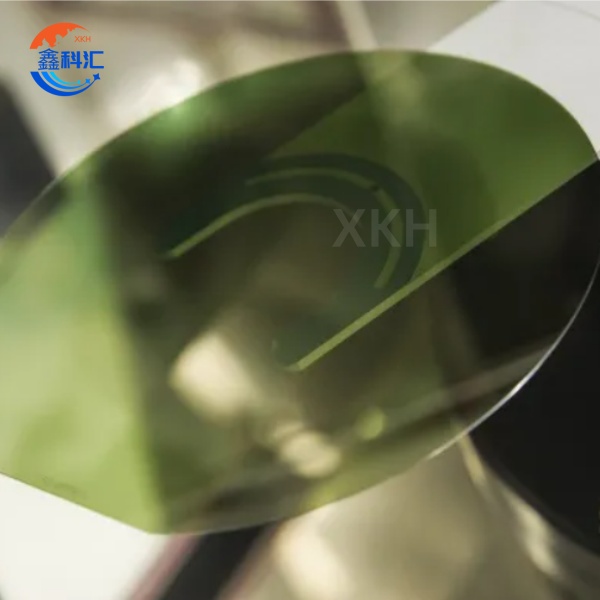
Customized SiC Seed Crystal Substrates Dia 205/203/208 4H-N Type for Optical Communications


Technical parameters
Silicon carbide seed wafer |
|
Polytype |
4H |
Surface orientation error |
4°toward<11-20>±0.5º |
Resistivity |
customization |
Diameter |
205±0.5mm |
Thickness |
600±50μm |
Roughness |
CMP,Ra≤0.2nm |
Micropipe Density |
≤1 ea/cm2 |
Scratches |
≤5,Total Length≤2*Diameter |
Edge chips/indents |
None |
Front laser marking |
None |
Scratches |
≤2,Total Length≤Diameter |
Edge chips/indents |
None |
Polytype areas |
None |
Back laser marking |
1mm (from top edge) |
Edge |
Chamfer |
Packaging |
Multi-wafer cassette |
Key Characteristics
1. Crystal Structure and Electrical Performance
· Crystallographic Stability: 100% 4H-SiC polytype dominance, zero multicrystalline inclusions (e.g., 6H/15R), with XRD rocking curve full-width at half-maximum (FWHM) ≤32.7 arcsec.
· High Carrier Mobility: Electron mobility of 5,400 cm²/V·s (4H-SiC) and hole mobility of 380 cm²/V·s, enabling high-frequency device designs.
·Radiation Hardness: Withstands 1 MeV neutron irradiation with a displacement damage threshold of 1×10¹⁵ n/cm², ideal for aerospace and nuclear applications.
2. Thermal and Mechanical Properties
· Exceptional Thermal Conductivity: 4.9 W/cm·K (4H-SiC), triple that of silicon, supporting operation above 200°C.
· Low Thermal Expansion Coefficient: CTE of 4.0×10⁻⁶/K (25–1000°C), ensuring compatibility with silicon-based packaging and minimizing thermal stress.
3. Defect Control and Processing Precision
· Micropipe Density: <0.3 cm⁻² (8-inch wafers), dislocation density <1,000 cm⁻² (verified via KOH etching).
· Surface Quality: CMP-polished to Ra <0.2 nm, meeting EUV lithography-grade flatness requirements.
Key Applications
|
Domain |
Application Scenarios |
Technical Advantages |
|
Optical Communications |
100G/400G lasers, silicon photonics hybrid modules |
InP seed substrates enable direct bandgap (1.34 eV) and Si-based heteroepitaxy, reducing optical coupling loss. |
|
New Energy Vehicles |
800V high-voltage inverters, onboard chargers (OBC) |
4H-SiC substrates withstand >1,200 V, reducing conduction losses by 50% and system volume by 40%. |
|
5G Communications |
Millimeter-wave RF devices (PA/LNA), base station power amplifiers |
Semi-insulating SiC substrates (resistivity >10⁵ Ω·cm) enable high-frequency (60 GHz+) passive integration. |
|
Industrial Equipment |
High-temperature sensors, current transformers, nuclear reactor monitors |
InSb seed substrates (0.17 eV bandgap) deliver magnetic sensitivity up to 300%@10 T. |
Key Advantages
SiC (silicon carbide) seed crystal substrates deliver unparalleled performance with 4.9 W/cm·K thermal conductivity, 2–4 MV/cm breakdown field strength, and 3.2 eV wide bandgap, enabling high-power, high-frequency, and high-temperature applications. Featuring zero micropipe density and <1,000 cm⁻² dislocation density, these substrates ensure reliability in extreme conditions. Their chemical inertness and CVD-compatible surfaces (Ra <0.2 nm) support advanced heteroepitaxial growth (e.g., SiC-on-Si) for optoelectronics and EV power systems.
XKH Services:
1. Customized Production
· Flexible Wafer Formats: 2–12-inch wafers with circular, rectangular, or custom-shaped cuts (±0.01 mm tolerance).
· Doping Control: Precise nitrogen (N) and aluminum (Al) doping via CVD, achieving resistivity ranges from 10⁻³ to 10⁶ Ω·cm.
2. Advanced Process Technologies
· Heteroepitaxy: SiC-on-Si (compatible with 8-inch silicon lines) and SiC-on-Diamond (thermal conductivity >2,000 W/m·K).
· Defect Mitigation: Hydrogen etching and annealing to reduce micropipe/density defects, improving wafer yield to >95%.
3. Quality Management Systems
· End-to-End Testing: Raman spectroscopy (polytype verification), XRD (crystallinity), and SEM (defect analysis).
· Certifications: Compliant with AEC-Q101 (automotive), JEDEC (JEDEC-033), and MIL-PRF-38534 (military-grade).
4. Global Supply Chain Support
· Production Capacity: Monthly output >10,000 wafers (60% 8-inch), with 48-hour emergency delivery.
· Logistics Network: Coverage in Europe, North America, and Asia-Pacific via air/sea freight with temperature-controlled packaging.
5. Technical Co-Development
· Joint R&D Labs: Collaborate on SiC power module packaging optimization (e.g., DBC substrate integration).
· IP Licensing: Provide GaN-on-SiC RF epitaxial growth technology licensing to reduce client R&D costs.
Summary
SiC (silicon carbide) seed crystal substrates, as a strategic material, are reshaping global industrial chains through breakthroughs in crystal growth, defect control, and heterogeneous integration. By continuously advancing wafer defect reduction, scaling 8-inch production, and expanding heteroepitaxial platforms (e.g., SiC-on-Diamond), XKH deliver high-reliability, cost-effective solutions for optoelectronics, new energy, and advanced manufacturing. Our commitment to innovation ensures clients lead in carbon neutrality and intelligent systems, driving the next era of wide-bandgap semiconductor ecosystems.
Related Products
-

150mm 6 inch 0.7mm 0.5mm Sapphire Wafer Substra...
-

Silicon Carbide Cantilever Paddle (SiC Cantilev...
-

156mm 159mm 6 inch Sapphire Wafer for carrier C...
-
Sapphire green for gemstone olive green artific...
-

p-type 4H/6H-P 3C-N TYPE SIC substrate 4inch ...
-

LiTaO3 Lithium Tantalate Ingots with Fe/Mg Dopi...