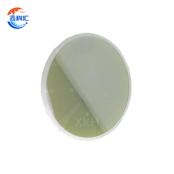
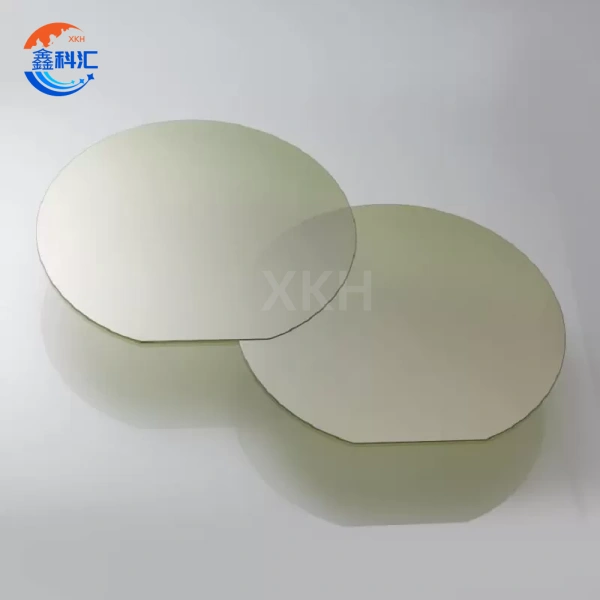
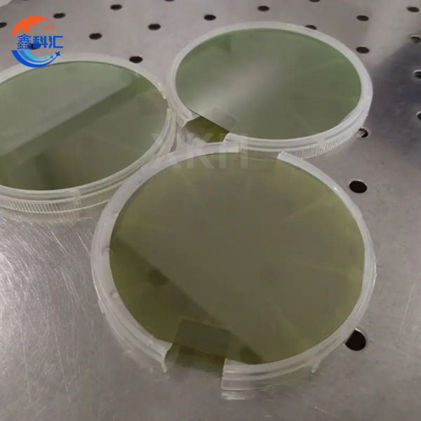
Custom N Type SiC Seed Substrate Dia153/155mm For Power Electronics


Introduce
Silicon Carbide (SiC) seed substrates serve as the foundational material for third-generation semiconductors, distinguished by their exceptionally high thermal conductivity, superior breakdown electric field strength, and high electron mobility. These properties make them indispensable for power electronics, RF devices, electric vehicles (EVs), and renewable energy applications. XKH specializes in the R&D and production of high-quality SiC seed substrates, employing advanced crystal growth techniques such as Physical Vapor Transport (PVT) and High-Temperature Chemical Vapor Deposition (HTCVD) to ensure industry-leading crystalline quality.
XKH offer 4-inch, 6-inch, and 8-inch SiC seed substrates with customizable N-type/P-type doping, achieving resistivity levels of 0.01-0.1 Ω·cm and dislocation densities below 500 cm⁻², making them ideal for manufacturing MOSFETs, Schottky Barrier Diodes (SBDs), and IGBTs. Our vertically integrated production process covers crystal growth, wafer slicing, polishing, and inspection, with a monthly production capacity exceeding 5,000 wafers to meet the diverse demands of research institutions, semiconductor manufacturers, and renewable energy companies.
Additionally, we provide custom solutions, including:
Crystal orientation customization (4H-SiC, 6H-SiC)
Specialized doping (Aluminum, Nitrogen, Boron, etc.)
Ultra-smooth polishing (Ra < 0.5 nm)
XKH support sample-based processing, technical consultations, and small-batch prototyping to deliver optimized SiC substrate solutions.
Technical parameters
| Silicon carbide seed wafer | |
| Polytype | 4H |
| Surface orientation error | 4°toward<11-20>±0.5º |
| Resistivity | customization |
| Diameter | 205±0.5mm |
| Thickness | 600±50μm |
| Roughness | CMP,Ra≤0.2nm |
| Micropipe Density | ≤1 ea/cm2 |
| Scratches | ≤5,Total Length≤2*Diameter |
| Edge chips/indents | None |
| Front laser marking | None |
| Scratches | ≤2,Total Length≤Diameter |
| Edge chips/indents | None |
| Polytype areas | None |
| Back laser marking | 1mm (from top edge) |
| Edge | Chamfer |
| Packaging | Multi-wafer cassette |
SiC Seed Substrates - Key Characteristics
1. Exceptional Physical Properties
· High thermal conductivity (~490 W/m·K), significantly surpassing silicon (Si) and gallium arsenide (GaAs), making it ideal for high-power-density device cooling.
· Breakdown field strength (~3 MV/cm), enabling stable operation under high-voltage conditions, critical for EV inverters and industrial power modules.
· Wide bandgap (3.2 eV), reducing leakage currents at high temperatures and enhancing device reliability.
2. Superior Crystalline Quality
· PVT + HTCVD hybrid growth technology minimizes micropipe defects, maintaining dislocation densities below 500 cm⁻².
· Wafer bow/warp < 10 μm and surface roughness Ra < 0.5 nm, ensuring compatibility with high-precision lithography and thin-film deposition processes.
3. Diverse Doping Options
·N-type (Nitrogen-doped): Low resistivity (0.01-0.02 Ω·cm), optimized for high-frequency RF devices.
· P-type (Aluminum-doped): Ideal for power MOSFETs and IGBTs, improving carrier mobility.
· Semi-insulating SiC (Vanadium-doped): Resistivity > 10⁵ Ω·cm, tailored for 5G RF front-end modules.
4. Environmental Stability
· High-temperature resistance (>1600°C) and radiation hardness, suitable for aerospace, nuclear equipment, and other extreme environments.
SiC Seed Substrates - Primary Applications
1. Power Electronics
· Electric Vehicles (EVs): Used in on-board chargers (OBC) and inverters to improve efficiency and reduce thermal management demands.
· Industrial Power Systems: Enhances photovoltaic inverters and smart grids, achieving >99% power conversion efficiency.
2. RF Devices
· 5G Base Stations: Semi-insulating SiC substrates enable GaN-on-SiC RF power amplifiers, supporting high-frequency, high-power signal transmission.
Satellite Communications: Low-loss characteristics make it suitable for millimeter-wave devices.
3. Renewable Energy & Energy Storage
· Solar Power: SiC MOSFETs boost DC-AC conversion efficiency while reducing system costs.
· Energy Storage Systems (ESS): Optimizes bidirectional converters and extends battery lifespan.
4. Defense & Aerospace
· Radar Systems: High-power SiC devices are used in AESA (Active Electronically Scanned Array) radars.
· Spacecraft Power Management: Radiation-resistant SiC substrates are critical for deep-space missions.
5. Research & Emerging Technologies
· Quantum Computing: High-purity SiC enables spin qubit research.
· High-Temperature Sensors: Deployed in oil exploration and nuclear reactor monitoring.
SiC Seed Substrates - XKH Services
1. Supply Chain Advantages
· Vertically integrated manufacturing: Full control from high-purity SiC powder to finished wafers, ensuring lead times of 4-6 weeks for standard products.
· Cost competitiveness: Economies of scale enable 15-20% lower pricing than competitors, with support for Long-Term Agreements (LTAs).
2. Customization Services
· Crystal orientation: 4H-SiC (standard) or 6H-SiC (specialized applications).
· Doping optimization: Tailored N-type/P-type/semi-insulating properties.
· Advanced polishing: CMP polishing and epi-ready surface treatment (Ra < 0.3 nm).
3. Technical Support
· Free sample testing: Includes XRD, AFM, and Hall effect measurement reports.
· Device simulation assistance: Supports epitaxial growth and device design optimization.
4. Rapid Response
· Low-volume prototyping: Minimum order of 10 wafers, delivered within 3 weeks.
· Global logistics: Partnerships with DHL and FedEx for door-to-door delivery.
5. Quality Assurance
· Full-process inspection: Covers X-ray topography (XRT) and defect density analysis.
· International certifications: Compliant with IATF 16949 (automotive-grade) and AEC-Q101 standards.
Conclusion
XKH's SiC seed substrates excel in crystalline quality, supply chain stability, and customization flexibility, serving power electronics, 5G communications, renewable energy, and defense technologies. We continue to advance 8-inch SiC mass-production technology to drive the third-generation semiconductor industry forward.


