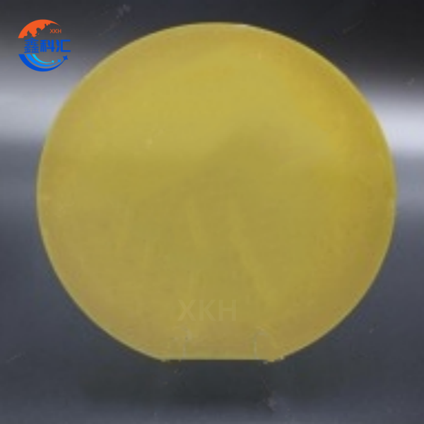
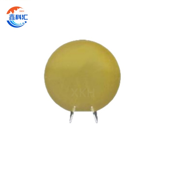
6 inch Conductive single crystal SiC on polycrystalline SiC composite substrate Diameter 150mm P type N type


Technical parameters
|
Size: |
6 inch |
|
Diameter: |
150 mm |
|
Thickness: |
400-500 μm |
|
Monocrystalline SiC Film Parameters |
|
|
Polytype: |
4H-SiC or 6H-SiC |
|
Doping Concentration: |
1×10¹⁴ - 1×10¹⁸ cm⁻³ |
|
Thickness: |
5-20 μm |
|
Sheet Resistance: |
10-1000 Ω/sq |
|
Electron Mobility: |
800-1200 cm²/Vs |
|
Hole Mobility: |
100-300 cm²/Vs |
|
Polycrystalline SiC Buffer Layer Parameters |
|
|
Thickness: |
50-300 μm |
|
Thermal Conductivity: |
150-300 W/m·K |
|
Monocrystalline SiC Substrate Parameters |
|
|
Polytype: |
4H-SiC or 6H-SiC |
|
Doping Concentration: |
1×10¹⁴ - 1×10¹⁸ cm⁻³ |
|
Thickness: |
300-500 μm |
|
Grain Size: |
> 1 mm |
|
Surface Roughness: |
< 0.3 mm RMS |
|
Mechanical & Electrical Properties |
|
|
Hardness: |
9-10 Mohs |
|
Compressive Strength: |
3-4 GPa |
|
Tensile Strength: |
0.3-0.5 GPa |
|
Breakdown Field Strength: |
> 2 MV/cm |
|
Total Dose Tolerance: |
> 10 Mrad |
|
Single Event Effect Resistance: |
> 100 MeV·cm²/mg |
|
Thermal Conductivity: |
150-380 W/m·K |
|
Operating Temperature Range: |
-55 to 600°C |
Key Characteristics
The 6-inch conductive monocrystalline SiC on polycrystalline SiC composite substrate offers a unique balance of material structure and performance, making it suitable for demanding industrial environments:
1.Cost-Effectiveness: The polycrystalline SiC base substantially reduces costs compared to full-monocrystalline SiC, while the monocrystalline SiC active layer ensures device-grade performance, ideal for cost-sensitive applications.
2.Exceptional Electrical Properties: The monocrystalline SiC layer exhibits high carrier mobility (>500 cm²/V·s) and low defect density, supporting high-frequency and high-power device operation.
3.High-Temperature Stability: SiC's inherent high-temperature resistance (>600°C) ensures the composite substrate remains stable under extreme conditions, making it suitable for electric vehicles and industrial motor applications.
4.6-inch Standardized Wafer Size: Compared to traditional 4-inch SiC substrates, the 6-inch format increases chip yield by over 30%, reducing per-unit device costs.
5.Conductive Design: Pre-doped N-type or P-type layers minimize ion implantation steps in device manufacturing, improving production efficiency and yield.
6.Superior Thermal Management: The polycrystalline SiC base's thermal conductivity (~120 W/m·K) approaches that of monocrystalline SiC, effectively addressing heat dissipation challenges in high-power devices.
These characteristics position the 6-inch conductive monocrystalline SiC on polycrystalline SiC composite substrate as a competitive solution for industries such as renewable energy, rail transportation, and aerospace.
Primary Applications
The 6-inch conductive monocrystalline SiC on polycrystalline SiC composite substrate has been successfully deployed in several high-demand fields:
1.Electric Vehicle Powertrains: Used in high-voltage SiC MOSFETs and diodes to enhance inverter efficiency and extend battery range (e.g., Tesla, BYD models).
2.Industrial Motor Drives: Enables high-temperature, high-switching-frequency power modules, reducing energy consumption in heavy machinery and wind turbines.
3.Photovoltaic Inverters: SiC devices improve solar conversion efficiency (>99%), while the composite substrate further reduces system costs.
4.Rail Transportation: Applied in traction converters for high-speed rail and subway systems, offering high-voltage resistance (>1700V) and compact form factors.
5.Aerospace: Ideal for satellite power systems and aircraft engine control circuits, capable of withstanding extreme temperatures and radiation.
In practical fabrication, the 6-inch conductive monocrystalline SiC on polycrystalline SiC composite substrate is fully compatible with standard SiC device processes (e.g., lithography, etching), requiring no additional capital investment.
XKH Services
XKH provide comprehensive support for the 6-inch conductive monocrystalline SiC on polycrystalline SiC composite substrate, covering R&D to mass production:
1.Customization: Adjustable monocrystalline layer thickness (5–100 μm), doping concentration (1e15–1e19 cm⁻³), and crystal orientation (4H/6H-SiC) to meet diverse device requirements.
2.Wafer Processing: Bulk supply of 6-inch substrates with backside thinning and metallization services for plug-and-play integration.
3.Technical Validation: Includes XRD crystallinity analysis, Hall effect testing, and thermal resistance measurement to expedite material qualification.
4.Rapid Prototyping: 2- to 4-inch samples (same process) for research institutions to accelerate development cycles.
5.Failure Analysis & Optimization: Material-level solutions for processing challenges (e.g., epitaxial layer defects).
Our mission is to establish the 6-inch conductive monocrystalline SiC on polycrystalline SiC composite substrate as the preferred cost-performance solution for SiC power electronics, offering end-to-end support from prototyping to volume production.
Conclusion
The 6-inch conductive monocrystalline SiC on polycrystalline SiC composite substrate achieves a breakthrough balance between performance and cost through its innovative mono/polycrystalline hybrid structure. As electric vehicles proliferate and Industry 4.0 advances, this substrate provides a reliable material foundation for next-generation power electronics. XKH welcome collaborations to further explore the potential of SiC technology.