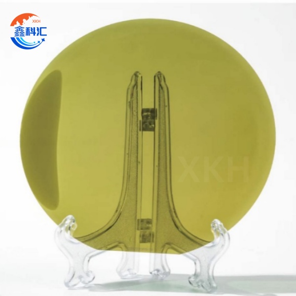
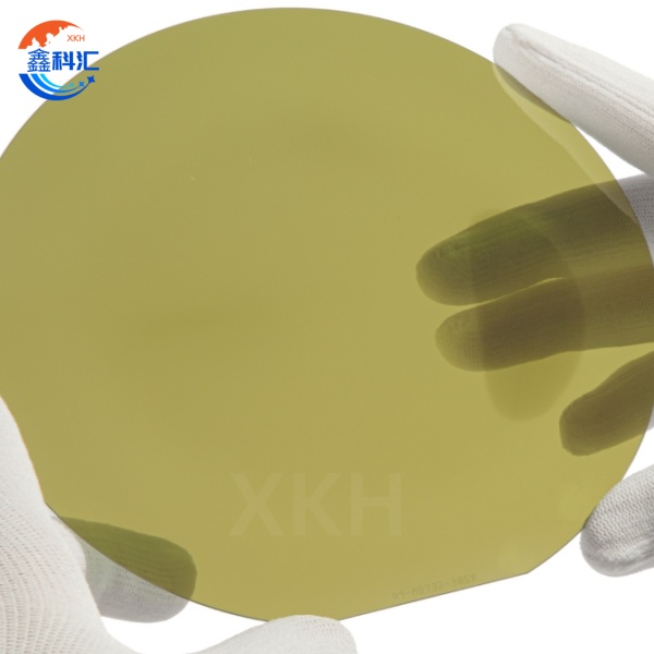
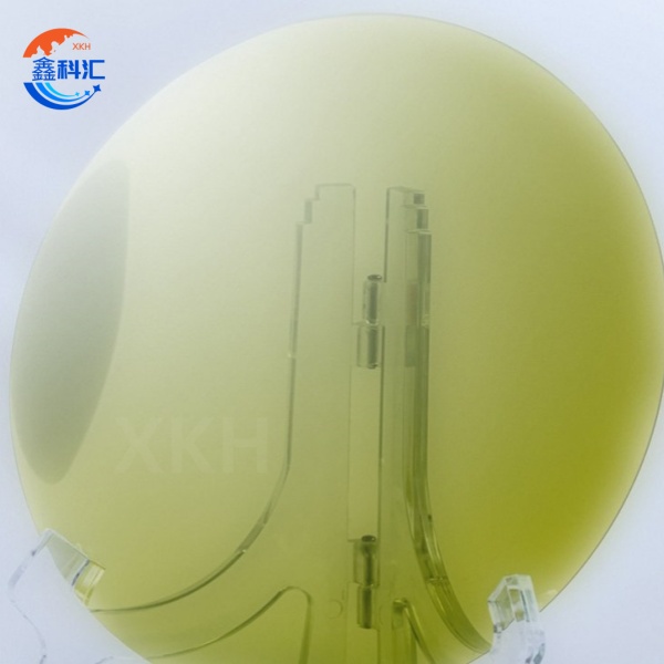
6 Inch Conductive SiC Composite Substrate 4H Diameter 150mm Ra≤0.2nm Warp≤35μm


Technical parameters
|
Items |
Production grade |
Dummy grade |
|
Diameter |
6-8 inch |
6-8 inch |
|
Thickness |
350/500±25.0 μm |
350/500±25.0 μm |
|
Polytype |
4H |
4H |
|
Resistivity |
0.015-0.025 ohm·cm |
0.015-0.025 ohm·cm |
|
TTV |
≤5 μm |
≤20 μm |
|
Warp |
≤35 μm |
≤55 μm |
|
Front (Si-face) roughness |
Ra≤0.2 nm (5μm×5μm) |
Ra≤0.2 nm (5μm×5μm) |
Key Features
1.Cost Advantage: Our 6-inch conductive SiC composite substrate employs proprietary "graded buffer layer" technology that optimizes material composition to reduce raw material costs by 38% while maintaining excellent electrical performance. Actual measurements show that 650V MOSFET devices using this substrate achieve a 42% reduction in cost per unit area compared to conventional solutions, which is significant for promoting SiC device adoption in consumer electronics.
2.Excellent Conductive Properties: Through precise nitrogen doping control processes, our 6-inch conductive SiC composite substrate achieves ultra-low resistivity of 0.012-0.022Ω·cm, with variation controlled within ±5%. Notably, we maintain resistivity uniformity even within the 5mm edge region of the wafer, solving a long-standing edge effect problem in the industry.
3.Thermal Performance: A 1200V/50A module developed using our substrate shows only 45℃ junction temperature rise above ambient at full load operation - 65℃ lower than comparable silicon-based devices. This is enabled by our "3D thermal channel" composite structure that improves lateral thermal conductivity to 380W/m·K and vertical thermal conductivity to 290W/m·K.
4.Process Compatibility: For the unique structure of 6-inch conductive SiC composite substrates, we developed a matching stealth laser dicing process achieving 200mm/s cutting speed while controlling edge chipping below 0.3μm. Additionally, we offer pre-nickel-plated substrate options that enable direct die bonding, saving customers two process steps.
Main Applications
Critical Smart Grid Equipment:
In ultra-high voltage direct current (UHVDC) transmission systems operating at ±800kV, IGCT devices utilizing our 6-inch conductive SiC composite substrates demonstrate remarkable performance enhancements. These devices achieve 55% reduction in switching losses during commutation processes, while increasing overall system efficiency to exceed 99.2%. The substrates' superior thermal conductivity (380W/m·K) enables compact converter designs that reduce substation footprint by 25% compared to conventional silicon-based solutions.
New Energy Vehicle Powertrains:
The drive system incorporating our 6-inch conductive SiC composite substrates achieves unprecedented inverter power density of 45kW/L - a 60% improvement over their previous 400V silicon-based design. Most impressively, the system maintains 98% efficiency across the entire operating temperature range from -40℃ to +175℃, solving the cold-weather performance challenges that have plagued EV adoption in northern climates. Real-world testing shows a 7.5% increase in winter range for vehicles equipped with this technology.
Industrial Variable Frequency Drives:
The adoption of our substrates in intelligent power modules (IPMs) for industrial servo systems is transforming manufacturing automation. In CNC machining centers, these modules deliver 40% faster motor response (reducing acceleration time from 50ms to 30ms) while cutting electromagnetic noise by 15dB to 65dB(A).
Consumer Electronics:
The consumer electronics revolution continues with our substrates enabling next-generation 65W GaN fast chargers. These compact power adapters achieve 30% volume reduction (down to 45cm³) while maintaining full power output, thanks to the superior switching characteristics of SiC-based designs. Thermal imaging shows maximum case temperatures of just 68°C during continuous operation - 22°C cooler than conventional designs - significantly improving product lifespan and safety.
XKH Customization Services
XKH provides comprehensive customization support for 6-inch conductive SiC composite substrates:
Thickness Customization: Options including 200μm, 300μm, and 350μm specifications
2. Resistivity Control: Adjustable n-type doping concentration from 1×10¹⁸ to 5×10¹⁸ cm⁻³
3. Crystal Orientation: Support for multiple orientations including (0001) off-axis 4° or 8°
4. Testing Services: Complete wafer-level parameter test reports
Our current lead time from prototyping to mass production can be as short as 8 weeks. For strategic customers, we offer dedicated process development services to ensure perfect matching with device requirements.