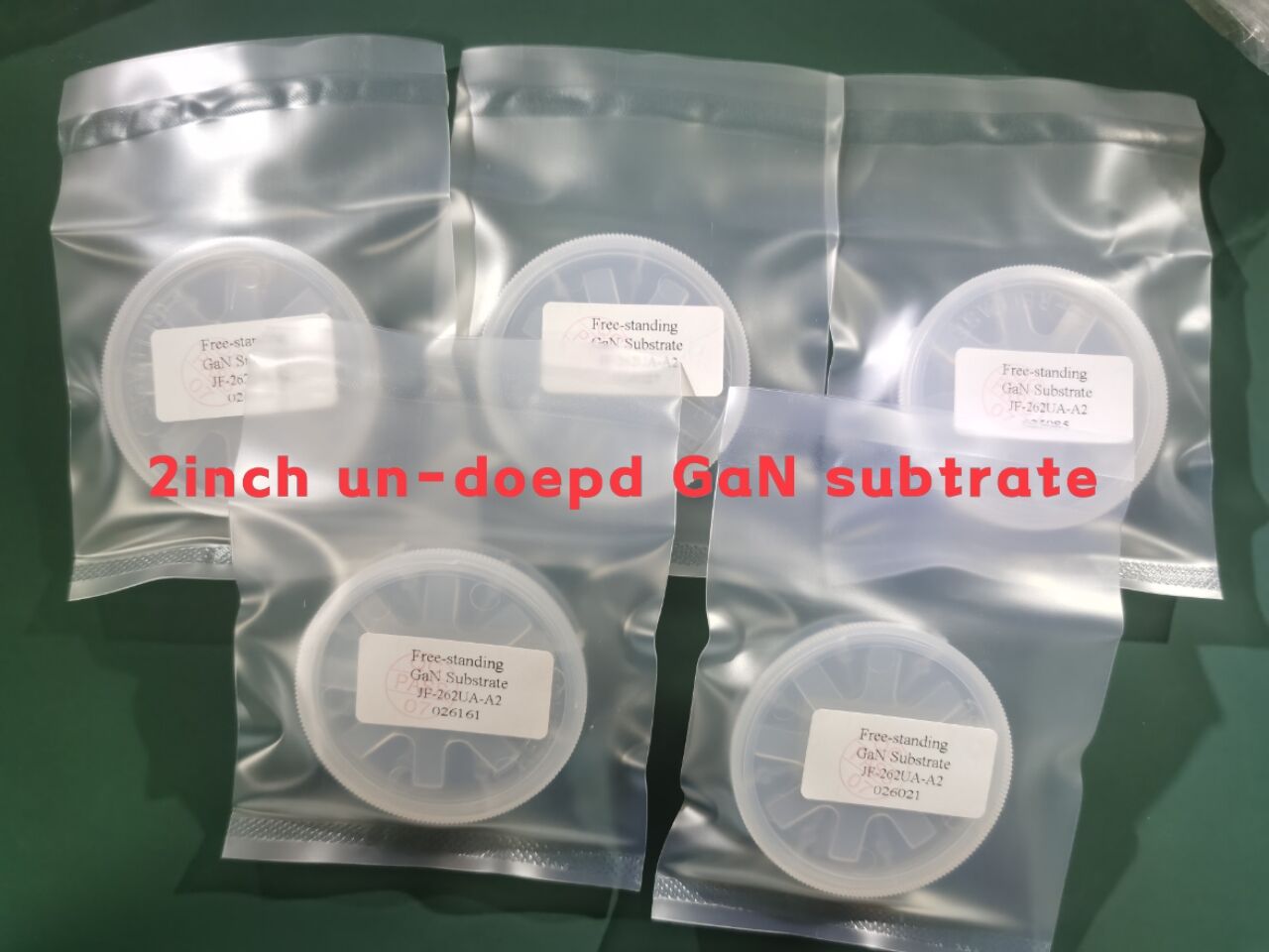
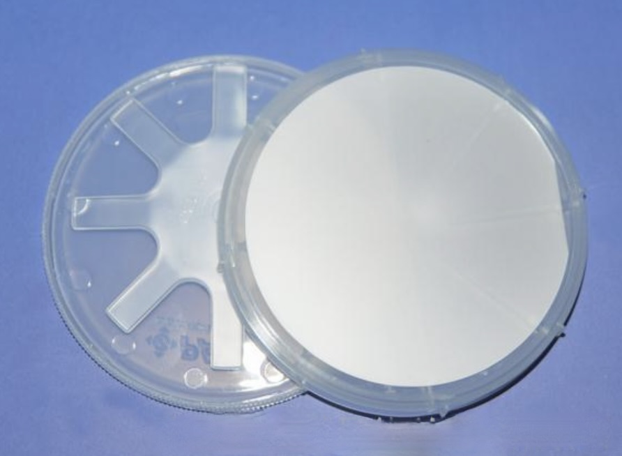
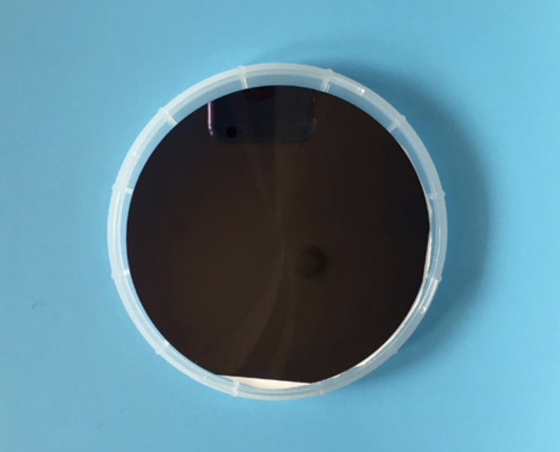
100mm 4inch GaN on Sapphire Epi-layer wafer Gallium nitride epitaxial wafer

The growth process of GaN blue LED quantum well structure. Detailed process flow is as follows
(1) High temperature baking, sapphire substrate is first heated to 1050℃ in a hydrogen atmosphere, the purpose is to clean the substrate surface;
(2) When the substrate temperature drops to 510℃, a low-temperature GaN/AlN buffer layer with a thickness of 30nm is deposited on the surface of the sapphire substrate;
(3) Temperature rise to 10 ℃, the reaction gas ammonia, trimethylgallium and silane are injected, respectively control the corresponding flow rate, and the silicon-doped N-type GaN of 4um thickness is grown;
(4) The reaction gas of trimethyl aluminum and trimethyl gallium was used to prepare silicon-doped N-type A⒑ continents with a thickness of 0.15um;
(5) 50nm Zn-doped InGaN was prepared by injecting trimethylgallium, trimethylindium, diethylzinc and ammonia at a temperature of 8O0℃ and controlling different flow rates respectively;
(6) The temperature was increased to 1020℃, trimethylaluminum, trimethylgallium and bis (cyclopentadienyl) magnesium were injected to prepare 0.15um Mg doped P-type AlGaN and 0.5um Mg doped P-type G blood glucose;
(7) High quality P-type GaN Sibuyan film was obtained by annealing in nitrogen atmosphere at 700℃;
(8) Etching on the P-type G stasis surface to reveal the N-type G stasis surface;
(9) Evaporation of Ni/Au contact plates on p-GaNI surface, evaporation of △/Al contact plates on ll-GaN surface to form electrodes.
Specifications
| Item |
GaN-T-C-U-C100 |
GaN-T-C-N-C100 |
| Dimensions |
e 100 mm ± 0.1 mm |
|
| Thickness |
4.5±0.5 um Can be customized |
|
| Orientation |
C-plane(0001) ±0.5° |
|
| Conduction Type |
N-type (Undoped) |
N-type (Si-doped) |
| Resistivity(300K) |
< 0.5 Q・cm |
< 0.05 Q・cm |
| Carrier Concentration |
< 5x1017 cm-3 |
> 1x1018 cm-3 |
| Mobility |
~ 300 cm2/V-s |
~ 200 cm2/V-s |
| Dislocation Density |
Less than 5x108 cm-2 (calculated by FWHMs of XRD) |
|
| Substrate structure |
GaN on Sapphire(Standard: SSP Option: DSP) |
|
| Useable Surface Area |
> 90% |
|
| Package |
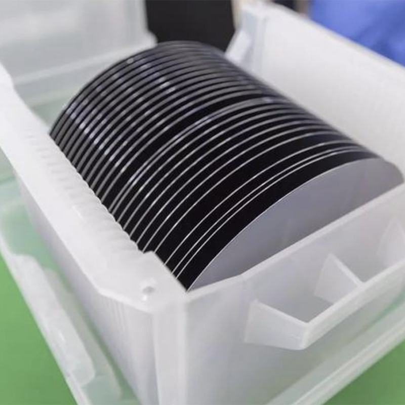
Packaged in a class 100 clean room environment, in cassettes of 25pcs or single wafer containers, under a nitrogen atmosphere. |
|
Detailed Diagram