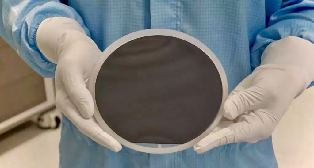
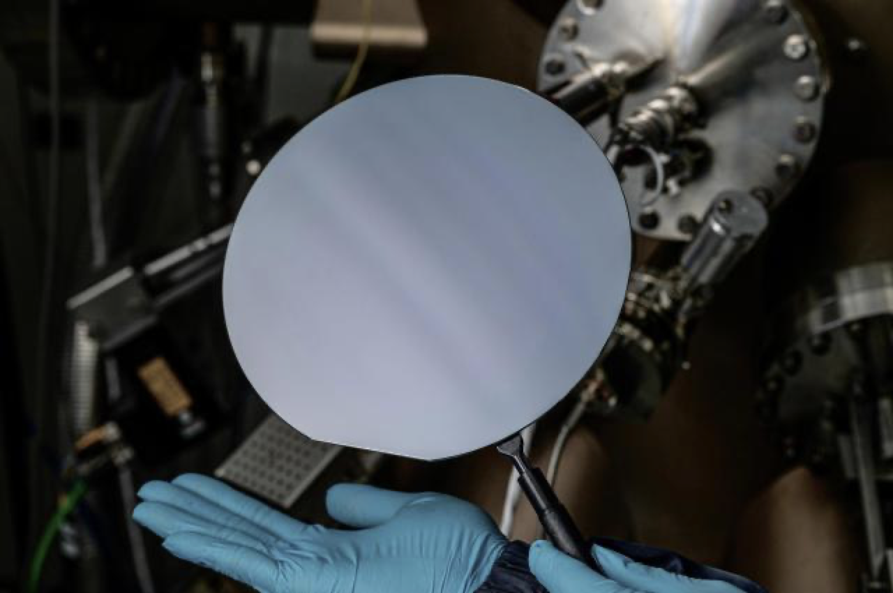
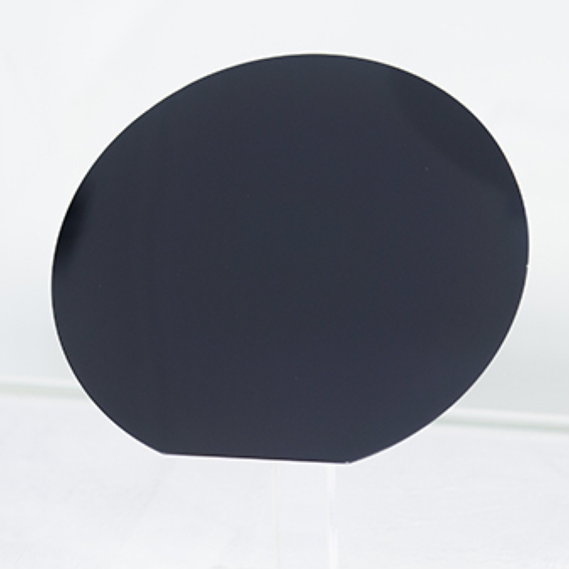
150mm 200mm 6inch 8inch GaN on Silicon Epi-layer wafer Gallium nitride epitaxial wafer


Manufacturing method
The manufacturing process involves growing GaN layers on a sapphire substrate using advanced techniques such as metal-organic chemical vapor deposition (MOCVD) or molecular beam epitaxy (MBE). The deposition process is carried out under controlled conditions to ensure high crystal quality and uniform film.
6inch GaN-On-Sapphire applications: 6-inch sapphire substrate chips are widely used in microwave communications, radar systems, wireless technology and optoelectronics.
Some common applications include
1. Rf power amplifier
2. LED lighting industry
3. Wireless network communication equipment
4. Electronic devices in high temperature environment
5. Optoelectronic devices
Product specifications
- Size: The substrate diameter is 6 inches (about 150 mm).
- Surface quality: The surface has been finely polished to provide excellent mirror quality.
- Thickness: The thickness of GaN layer can be customized according to specific requirements.
- Packaging: The substrate is carefully packed with anti-static materials to prevent damage during transportation.
- Positioning edges: The substrate has specific positioning edges that facilitate alignment and operation during device preparation.
- Other parameters: Specific parameters such as thinness, resistivity and doping concentration can be adjusted according to customer requirements.
With their superior material properties and diverse applications, 6-inch sapphire substrate wafers are a reliable choice for the development of high-performance semiconductor devices in various industries.
|
Substrate |
6” 1mm <111> p-type Si |
6” 1mm <111> p-type Si |
|
Epi ThickAvg |
~5um |
~7um |
|
Epi ThickUnif |
<2% |
<2% |
|
Bow |
+/-45um |
+/-45um |
|
Cracking |
<5mm |
<5mm |
|
Vertical BV |
>1000V |
>1400V |
|
HEMT Al% |
25-35% |
25-35% |
|
HEMT ThickAvg |
20-30nm |
20-30nm |
|
Insitu SiN Cap |
5-60nm |
5-60nm |
|
2DEG conc. |
~1013cm-2 |
~1013cm-2 |
|
Mobility |
~2000cm2/Vs (<2%) |
~2000cm2/Vs (<2%) |
|
Rsh |
<330ohm/sq (<2%) |
<330ohm/sq (<2%) |
Detailed Diagram