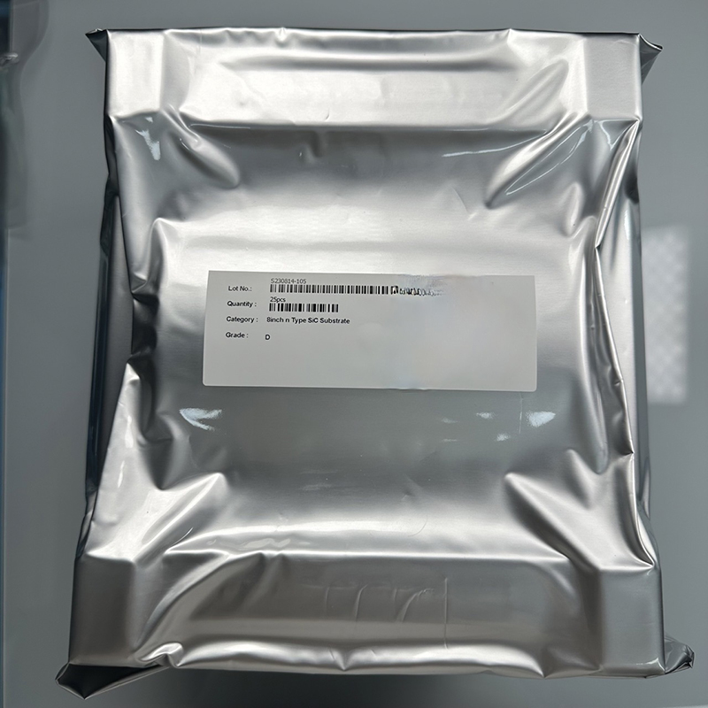
SiO₂ Quartz Wafer Quartz Wafers SiO₂ MEMS Temperature 2″ 3″ 4″ 6″ 8″ 12″


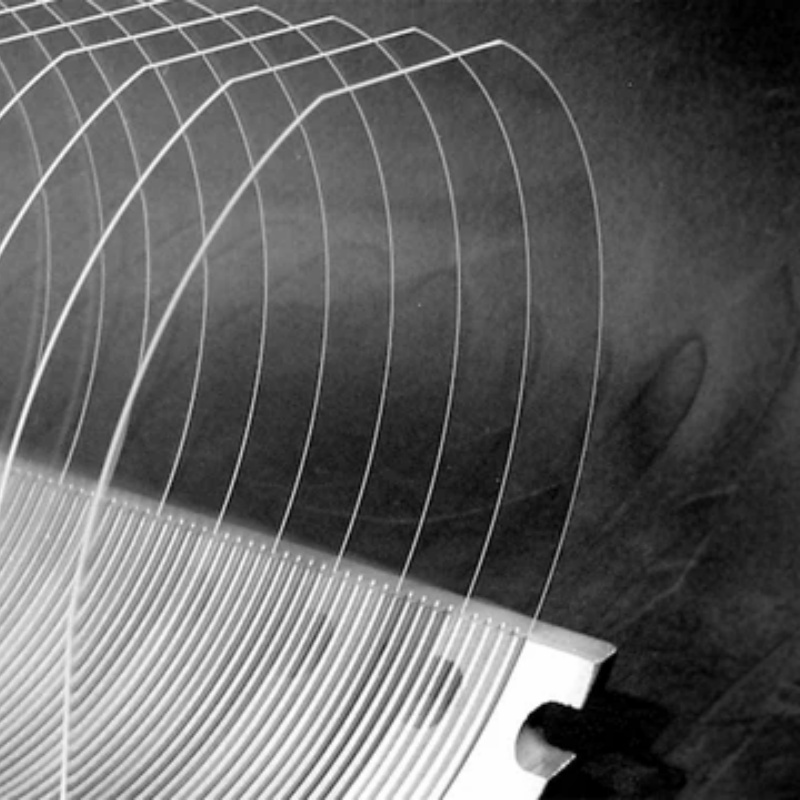
Detailed Diagram

Introduction
Quartz wafers play an indispensable role in advancing the electronics, semiconductor, and optics industries. Found in smartphones guiding your GPS, embedded in high-frequency base stations powering 5G networks, and integrated into tools manufacturing next-gen microchips, quartz wafers are essential. These high-purity substrates enable innovations in everything from quantum computing to advanced photonics. Despite being derived from one of Earth's most abundant minerals, quartz wafers are engineered to extraordinary standards of precision and performance.

What Are Quartz Wafers
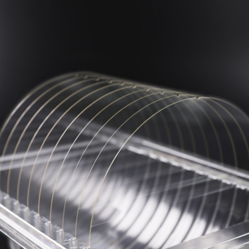
Quartz wafers are thin, circular discs created from ultra-pure synthetic quartz crystal. Available in standard diameters ranging from 2 to 12 inches, quartz wafers typically range in thickness from 0.5 mm to 6 mm. Unlike natural quartz, which forms irregular prismatic crystals, synthetic quartz is grown under tightly controlled lab conditions, producing uniform crystal structures.
The inherent crystallinity of quartz wafers provides unmatched chemical resistance, optical transparency, and stability under high temperature and mechanical stress. These features make quartz wafers a foundational component for precision devices used in data transmission, sensing, computation, and laser-based technologies.
Quartz Wafer Specifications
| Quartz Type | 4 | 6 | 8 | 12 |
|---|---|---|---|---|
| Size | ||||
| Diameter (inch) | 4 | 6 | 8 | 12 |
| Thickness (mm) | 0.05–2 | 0.25–5 | 0.3–5 | 0.4–5 |
| Diameter Tolerance (inch) | ±0.1 | ±0.1 | ±0.1 | ±0.1 |
| Thickness Tolerance (mm) | Customizable | Customizable | Customizable | Customizable |
| Optical Properties | ||||
| Refractive Index @365 nm | 1.474698 | 1.474698 | 1.474698 | 1.474698 |
| Refractive Index @546.1 nm | 1.460243 | 1.460243 | 1.460243 | 1.460243 |
| Refractive Index @1014 nm | 1.450423 | 1.450423 | 1.450423 | 1.450423 |
| Internal Transmittance (1250–1650 nm) | >99.9% | >99.9% | >99.9% | >99.9% |
| Total Transmittance (1250–1650 nm) | >92% | >92% | >92% | >92% |
| Machining Quality | ||||
| TTV (Total Thickness Variation, µm) | <3 | <3 | <3 | <3 |
| Flatness (µm) | ≤15 | ≤15 | ≤15 | ≤15 |
| Surface Roughness (nm) | ≤1 | ≤1 | ≤1 | ≤1 |
| Bow (µm) | <5 | <5 | <5 | <5 |
| Physical Properties | ||||
| Density (g/cm³) | 2.20 | 2.20 | 2.20 | 2.20 |
| Young's Modulus (GPa) | 74.20 | 74.20 | 74.20 | 74.20 |
| Mohs Hardness | 6–7 | 6–7 | 6–7 | 6–7 |
| Shear Modulus (GPa) | 31.22 | 31.22 | 31.22 | 31.22 |
| Poisson's Ratio | 0.17 | 0.17 | 0.17 | 0.17 |
| Compressive Strength (GPa) | 1.13 | 1.13 | 1.13 | 1.13 |
| Tensile Strength (MPa) | 49 | 49 | 49 | 49 |
| Dielectric Constant (1 MHz) | 3.75 | 3.75 | 3.75 | 3.75 |
| Thermal Properties | ||||
| Strain Point (10¹⁴.⁵ Pa·s) | 1000°C | 1000°C | 1000°C | 1000°C |
| Annealing Point (10¹³ Pa·s) | 1160°C | 1160°C | 1160°C | 1160°C |
| Softening Point (10⁷.⁶ Pa·s) | 1620°C | 1620°C | 1620°C | 1620°C |
Applications of Quartz Wafers
Quartz wafers are custom-engineered to meet demanding applications across industries including:
Electronics and RF Devices
- Quartz wafers are core to quartz crystal resonators and oscillators that provide clock signals for smartphones, GPS units, computers, and wireless communication devices.
- Their low thermal expansion and high Q-factor make quartz wafers perfect for high-stability timing circuits and RF filters.
Optoelectronics and Imaging
- Quartz wafers offer excellent UV and IR transmittance, making them ideal for optical lenses, beam splitters, laser windows, and detectors.
- Their resistance to radiation enables use in high-energy physics and space instruments.
Semiconductor and MEMS
- Quartz wafers serve as substrates for high-frequency semiconductor circuits, especially in GaN and RF applications.
- In MEMS (Micro-Electro-Mechanical Systems), quartz wafers convert mechanical signals into electrical ones via the piezoelectric effect, enabling sensors like gyroscopes and accelerometers.
Advanced Manufacturing & Labs
- High-purity quartz wafers are widely used in chemical, biomedical, and photonic labs for optical cells, UV cuvettes, and high-temp sample handling.
- Their compatibility with extreme environments makes them suitable for plasma chambers and deposition tools.
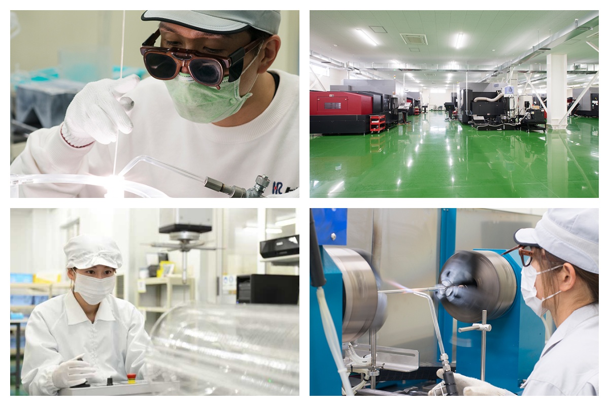
How Quartz Wafers Are Made
There are two primary manufacturing routes for quartz wafers:
Fused Quartz Wafers
Fused quartz wafers are made by melting natural quartz granules into an amorphous glass, then slicing and polishing the solid block into thin wafers. These quartz wafers offer:
- Exceptional UV transparency
- Wide thermal operating range (>1100°C)
- Excellent thermal shock resistance
They are ideal for lithography equipment, high-temperature furnaces, and optical windows but are not suitable for piezoelectric applications due to the lack of crystalline order.
Cultured Quartz Wafers
Cultured quartz wafers are grown synthetically to produce defect-free crystals with precise lattice orientation. These wafers are engineered for applications requiring:
- Exact cut angles (X-, Y-, Z-, AT-cut, etc.)
- High-frequency oscillators and SAW filters
- Optical polarizers and advanced MEMS devices
The production process involves seeded growth in autoclaves, followed by slicing, orientation, annealing, and polishing.
Leading Quartz Wafer Suppliers
Global suppliers specializing in high-precision quartz wafers include:
- Heraeus (Germany) – fused and synthetic quartz
- Shin-Etsu Quartz (Japan) – high-purity wafer solutions
- WaferPro (USA) – wide diameter quartz wafers and substrates
- Korth Kristalle (Germany) – synthetic crystal wafers
The Evolving Role of Quartz Wafers
Quartz wafers continue to evolve as essential components in emerging tech landscapes:
- Miniaturization – Quartz wafers are being fabricated with tighter tolerances for compact device integration.
- Higher Frequency Electronics – New quartz wafer designs are pushing into mmWave and THz domains for 6G and radar.
- Next-Gen Sensing – From autonomous vehicles to industrial IoT, quartz-based sensors are becoming more vital.
Frequently asked questions about quartz wafers
1. What is a quartz wafer?
A quartz wafer is a thin, flat disc made from crystalline silicon dioxide (SiO₂), typically manufactured in standard semiconductor sizes (e.g., 2", 3", 4", 6", 8", or 12"). Known for its high purity, thermal stability, and optical transparency, a quartz wafer is used as a substrate or carrier in various high-precision applications such as semiconductor fabrication, MEMS devices, optical systems, and vacuum processes.
2. What is the difference between quartz and silica gel?
Quartz is a crystalline solid form of silicon dioxide (SiO₂), while silica gel is an amorphous and porous form of SiO₂, commonly used as a desiccant to absorb moisture.
- Quartz is hard, transparent, and used in electronic, optical, and industrial applications.
- Silica gel appears as small beads or granules and is primarily used for humidity control in packaging, electronics, and storage.
3. What are quartz crystals used for?
Quartz crystals are widely used in electronics and optics due to their piezoelectric properties (they generate an electric charge under mechanical stress). Common applications include:
- Oscillators and frequency control (e.g., quartz watches, clocks, microcontrollers)
- Optical components (e.g., lenses, waveplates, windows)
- Resonators and filters in RF and communication devices
- Sensors for pressure, acceleration, or force
- Semiconductor fabrication as substrates or process windows
4. Why is quartz used in microchips?
Quartz is used in microchip-related applications because it offers:
- Thermal stability during high-temperature processes like diffusion and annealing
- Electrical insulation due to its dielectric properties
- Chemical resistance to acids and solvents used in semiconductor fabrication
- Dimensional precision and low thermal expansion for reliable lithography alignment
- While quartz itself isn't used as the active semiconductor material (like silicon), it plays a vital supporting role in the fabrication environment—especially in furnaces, chambers, and photomask substrates.
About Us
XKH specializes in high-tech development, production, and sales of special optical glass and new crystal materials. Our products serve optical electronics, consumer electronics, and the military. We offer Sapphire optical components, mobile phone lens covers, Ceramics, LT, Silicon Carbide SIC, Quartz, and semiconductor crystal wafers. With skilled expertise and cutting-edge equipment, we excel in non-standard product processing, aiming to be a leading optoelectronic materials high-tech enterprise.