SICOI (Silicon Carbide on Insulator) Wafers SiC Film ON Silicon


Detailed Diagram
Introduce of Silicon Carbide on Insulator (SICOI) wafers
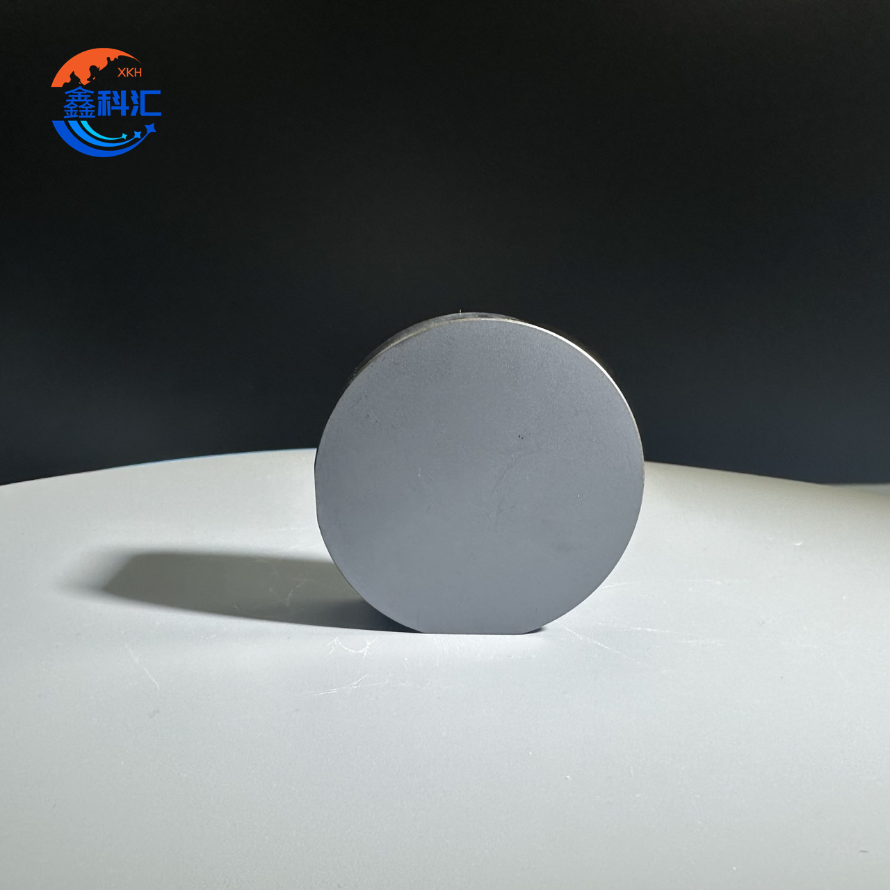
Silicon Carbide on Insulator (SICOI) wafers are next-generation semiconductor substrates that integrate the superior physical and electronic properties of silicon carbide (SiC) with the outstanding electrical isolation characteristics of an insulating buffer layer, such as silicon dioxide (SiO₂) or silicon nitride (Si₃N₄). A typical SICOI wafer consists of a thin epitaxial SiC layer, an intermediate insulating film, and a supporting base substrate, which can be either silicon or SiC.
This hybrid structure is engineered to meet the stringent demands of high-power, high-frequency, and high-temperature electronic devices. By incorporating an insulating layer, SICOI wafers minimize parasitic capacitance and suppress leakage currents, thereby ensuring higher operating frequencies, better efficiency, and improved thermal management. These benefits make them highly valuable in sectors such as electric vehicles, 5G telecommunication infrastructure, aerospace systems, advanced RF electronics, and MEMS sensor technologies.
Production Principle of SICOI Wafers
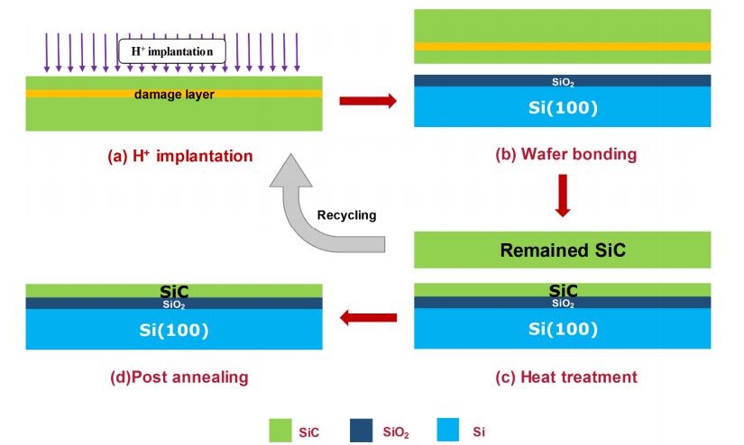
SICOI (Silicon Carbide on Insulator) wafers are manufactured through an advanced wafer bonding and thinning process:
-
SiC Substrate Growth – A high-quality single-crystal SiC wafer (4H/6H) is prepared as the donor material.
-
Insulating Layer Deposition – An insulating film (SiO₂ or Si₃N₄) is formed on the carrier wafer (Si or SiC).
-
Wafer Bonding – The SiC wafer and the carrier wafer are bonded together under high temperature or plasma assistance.
-
Thinning & Polishing – The SiC donor wafer is thinned down to a few micrometers and polished to achieve an atomically smooth surface.
-
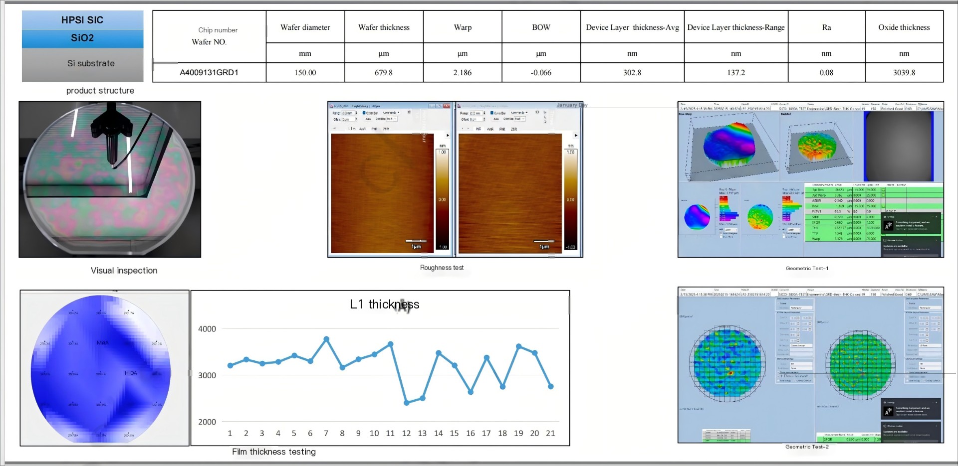
Final Inspection – The completed SICOI wafer is tested for thickness uniformity, surface roughness, and insulation performance.
Through this process, a thin active SiC layer with excellent electrical and thermal properties is combined with an insulating film and a support substrate, creating a high-performance platform for next-generation power and RF devices.
Key Advantages of SICOI Wafers
| Feature Category | Technical Characteristics | Core Benefits |
|---|---|---|
| Material Structure | 4H/6H-SiC active layer + insulating film (SiO₂/Si₃N₄) + Si or SiC carrier | Achieves strong electrical isolation, reduces parasitic interference |
| Electrical Properties | High breakdown strength (>3 MV/cm), low dielectric loss | Optimized for high-voltage and high-frequency operation |
| Thermal Properties | Thermal conductivity up to 4.9 W/cm·K, stable above 500°C | Effective heat dissipation, excellent performance under harsh thermal loads |
| Mechanical Properties | Extreme hardness (Mohs 9.5), low coefficient of thermal expansion | Robust against stress, enhances device longevity |
| Surface Quality | Ultra-smooth surface (Ra <0.2 nm) | Promotes defect-free epitaxy and reliable device fabrication |
| Insulation | Resistivity >10¹⁴ Ω·cm, low leakage current | Reliable operation in RF and high-voltage isolation applications |
| Size & Customization | Available in 4, 6, and 8-inch formats; SiC thickness 1–100 μm; insulation 0.1–10 μm | Flexible design for different application requirements |
Core Application Areas
| Application Sector | Typical Use Cases | Performance Advantages |
|---|---|---|
| Power Electronics | EV inverters, charging stations, industrial power devices | High breakdown voltage, reduced switching loss |
| RF & 5G | Base station power amplifiers, millimeter-wave components | Low parasitics, supports GHz-range operations |
| MEMS Sensors | Harsh-environment pressure sensors, navigation-grade MEMS | High thermal stability, resistant to radiation |
| Aerospace & Defense | Satellite communications, avionics power modules | Reliability in extreme temperatures and radiation exposure |
| Smart Grid | HVDC converters, solid-state circuit breakers | High insulation minimizes power loss |
| Optoelectronics | UV LEDs, laser substrates | High crystalline quality supports efficient light emission |


Fabrication of 4H-SiCOI
The production of 4H-SiCOI wafers is achieved through wafer bonding and thinning processes, enabling high-quality insulating interfaces and defect-free SiC active layers.
-
a: Schematic of the 4H-SiCOI material platform fabrication.
-
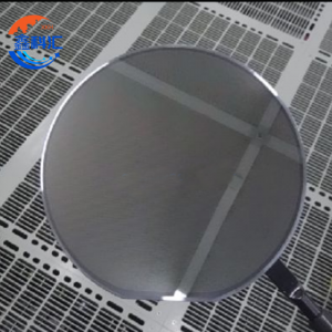
b: Image of a 4-inch 4H-SiCOI wafer using bonding and thinning; defect zones marked.
-
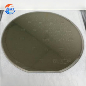
c: Thickness uniformity characterization of the 4H-SiCOI substrate.
-
d: Optical image of a 4H-SiCOI die.
-
e: Process flow for fabricating a SiC microdisk resonator.
-
f: SEM of a completed microdisk resonator.
-
g: Enlarged SEM showing resonator sidewall; AFM inset depicts nanoscale surface smoothness.
-
h: Cross-sectional SEM illustrating parabolic-shaped upper surface.
FAQ on SICOI Wafers
Q1: What advantages do SICOI wafers have over traditional SiC wafers?
A1: Unlike standard SiC substrates, SICOI wafers include an insulating layer that reduces parasitic capacitance and leakage currents, leading to higher efficiency, better frequency response, and superior thermal performance.
Q2: What wafer sizes are typically available?
A2: SICOI wafers are commonly produced in 4-inch, 6-inch, and 8-inch formats, with customized SiC and insulating layer thickness available depending on device requirements.
Q3: Which industries benefit the most from SICOI wafers?
A3: Key industries include power electronics for electric vehicles, RF electronics for 5G networks, MEMS for aerospace sensors, and optoelectronics such as UV LEDs.
Q4: How does the insulating layer improve device performance?
A4: The insulating film (SiO₂ or Si₃N₄) prevents current leakage and reduces electrical cross-talk, enabling higher voltage endurance, more efficient switching, and reduced heat loss.
Q5: Are SICOI wafers suitable for high-temperature applications?
A5: Yes, with high thermal conductivity and resistance beyond 500°C, SICOI wafers are designed to function reliably under extreme heat and in harsh environments.
Q6: Can SICOI wafers be customized?
A6: Absolutely. Manufacturers offer tailored designs for specific thicknesses, doping levels, and substrate combinations to meet diverse research and industrial needs.