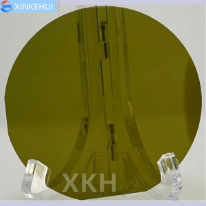
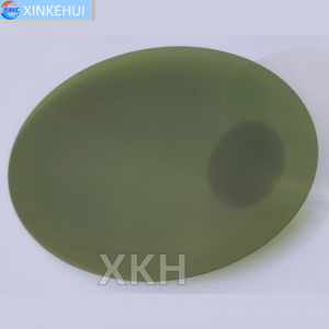
SiC Epitaxial Wafer for Power Devices – 4H-SiC, N-type, Low Defect Density


Detailed Diagram
Introduction
The SiC Epitaxial Wafer is at the core of modern high-performance semiconductor devices, especially those designed for high-power, high-frequency, and high-temperature operations. Short for Silicon Carbide Epitaxial Wafer, a SiC Epitaxial Wafer consists of a high-quality, thin SiC epitaxial layer grown atop a bulk SiC substrate. The use of SiC Epitaxial Wafer technology is rapidly expanding in electric vehicles, smart grids, renewable energy systems, and aerospace due to its superior physical and electronic properties compared to conventional silicon-based wafers.
Fabrication Principles of SiC Epitaxial Wafer
Creating a SiC Epitaxial Wafer requires a highly controlled chemical vapor deposition (CVD) process. The epitaxial layer is typically grown on a monocrystalline SiC substrate using gases such as silane (SiH₄), propane (C₃H₈), and hydrogen (H₂) at temperatures exceeding 1500°C. This high-temperature epitaxial growth ensures excellent crystalline alignment and minimal defects between the epitaxial layer and the substrate.
The process includes several key stages:
-
Substrate Preparation: The base SiC wafer is cleaned and polished to atomic smoothness.
-
CVD Growth: In a high-purity reactor, gases react to deposit a single-crystal SiC layer on the substrate.
-
Doping Control: N-type or P-type doping is introduced during epitaxy to achieve desired electrical properties.
-
Inspection and Metrology: Optical microscopy, AFM, and X-ray diffraction are used to verify layer thickness, doping concentration, and defect density.
Each SiC Epitaxial Wafer is carefully monitored to maintain tight tolerances in thickness uniformity, surface flatness, and resistivity. The ability to fine-tune these parameters is essential for high-voltage MOSFETs, Schottky diodes, and other power devices.
Specification
| Parameter | Specification |
| Categories | Materials Science, Single Crystal Substrates |
| Polytype | 4H |
| Doping | N Type |
| Diameter | 101 mm |
| Diameter Tolerance | ± 5% |
| Thickness | 0.35 mm |
| Thickness Tolerance | ± 5% |
| Primary Flat Length | 22 mm (± 10%) |
| TTV (Total Thickness Variation) | ≤10 µm |
| Warp | ≤25 µm |
| FWHM | ≤30 Arc-sec |
| Surface Finish | Rq ≤0.35 nm |
Applications of SiC Epitaxial Wafer
SiC Epitaxial Wafer products are indispensable in multiple sectors:
-
Electric Vehicles (EVs): SiC Epitaxial Wafer-based devices increase powertrain efficiency and reduce weight.
-
Renewable Energy: Used in inverters for solar and wind power systems.
-
Industrial Power Supplies: Enable high-frequency, high-temperature switching with lower losses.
-
Aerospace and Defense: Ideal for harsh environments requiring robust semiconductors.
-
5G Base Stations: SiC Epitaxial Wafer components support higher power densities for RF applications.
The SiC Epitaxial Wafer enables compact designs, faster switching, and higher energy conversion efficiency compared to silicon wafers.
Advantages of SiC Epitaxial Wafer
SiC Epitaxial Wafer technology offers significant benefits:
-
High Breakdown Voltage: Withstands voltages up to 10 times higher than Si wafers.
-
Thermal Conductivity: SiC Epitaxial Wafer dissipates heat faster, allowing devices to run cooler and more reliably.
-
High Switching Speeds: Lower switching losses enable higher efficiency and miniaturization.
-
Wide Bandgap: Ensures stability at higher voltages and temperatures.
-
Material Robustness: SiC is chemically inert and mechanically strong, ideal for demanding applications.
These advantages make the SiC Epitaxial Wafer the material of choice for the next generation of semiconductors.
FAQ: SiC Epitaxial Wafer
Q1: What is the difference between a SiC wafer and a SiC Epitaxial Wafer?
A SiC wafer refers to the bulk substrate, while a SiC Epitaxial Wafer includes a specially grown doped layer used in device fabrication.
Q2: What thicknesses are available for SiC Epitaxial Wafer layers?
Epitaxial layers typically range from a few micrometers to over 100 μm, depending on application requirements.
Q3: Is SiC Epitaxial Wafer suitable for high-temperature environments?
Yes, SiC Epitaxial Wafer can operate in conditions above 600°C, outperforming silicon significantly.
Q4: Why is defect density important in SiC Epitaxial Wafer?
Lower defect density improves device performance and yield, especially for high-voltage applications.
Q5: Are N-type and P-type SiC Epitaxial Wafers both available?
Yes, both types are produced using precise dopant gas control during the epitaxial process.
Q6: What wafer sizes are standard for SiC Epitaxial Wafer?
Standard diameters include 2-inch, 4-inch, 6-inch, and increasingly 8-inch for high-volume manufacturing.
Q7: How does SiC Epitaxial Wafer impact cost and efficiency?
While initially more expensive than silicon, SiC Epitaxial Wafer reduces system size and power loss, improving total cost efficiency over the long term.


