Semiconductor Laser Lift-Off Equipment


Detailed Diagram
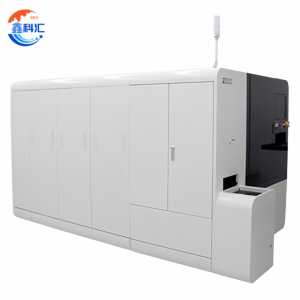
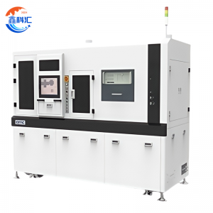
Product Overview of Laser Lift-Off Equipment
The Semiconductor Laser Lift-Off Equipment represents a next-generation solution for advanced ingot thinning in semiconductor material processing. Unlike traditional wafering methods that rely on mechanical grinding, diamond wire sawing, or chemical-mechanical planarization, this laser-based platform offers a contact-free, non-destructive alternative for detaching ultra-thin layers from bulk semiconductor ingots.
Optimized for brittle and high-value materials such as gallium nitride (GaN), silicon carbide (SiC), sapphire, and gallium arsenide (GaAs), the Semiconductor Laser Lift-Off Equipment enables precision slicing of wafer-scale films directly from the crystal ingot. This breakthrough technology significantly reduces material waste, improves throughput, and enhances substrate integrity — all of which are critical for next-generation devices in power electronics, RF systems, photonics, and micro-displays.
With an emphasis on automated control, beam shaping, and laser-material interaction analytics, the Semiconductor Laser Lift-Off Equipment is designed to seamlessly integrate into semiconductor fabrication workflows while supporting R&D flexibility and mass production scalability.
Technology & Operating Principle of Laser Lift-Off Equipment
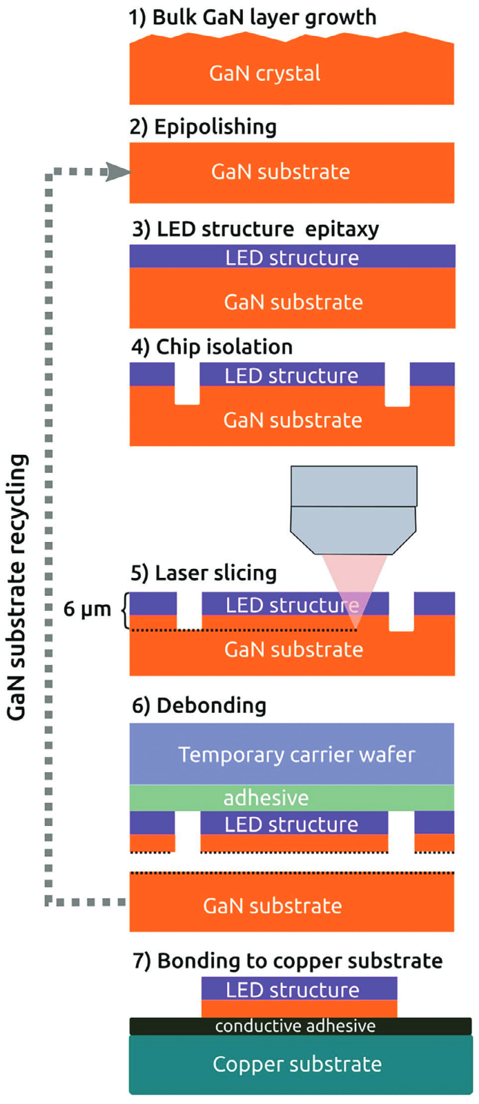
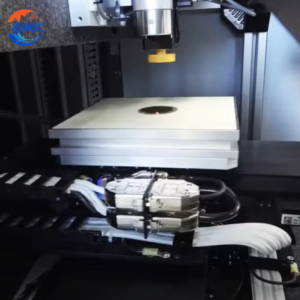
The process performed by Semiconductor Laser Lift-Off Equipment begins by irradiating the donor ingot from one side using a high-energy ultraviolet laser beam. This beam is tightly focused on a specific internal depth, typically along an engineered interface, where the energy absorption is maximized due to optical, thermal, or chemical contrast.
At this energy absorption layer, localized heating leads to a rapid micro-explosion, gas expansion, or decomposition of an interfacial layer (e.g., a stressor film or sacrificial oxide). This precisely controlled disruption causes the upper crystalline layer — with a thickness of tens of micrometers — to detach from the base ingot cleanly.
The Semiconductor Laser Lift-Off Equipment leverages motion-synchronized scanning heads, programmable z-axis control, and real-time reflectometry to ensure every pulse delivers energy exactly at the target plane. The equipment can also be configured with burst-mode or multi-pulse capabilities to enhance detachment smoothness and minimize residual stress. Importantly, because the laser beam never contacts the material physically, the risk of microcracking, bowing, or surface chipping is drastically reduced.
This makes the laser lift-off thinning method a game-changer, particularly in applications where ultra-flat, ultra-thin wafers are required with sub-micron TTV (Total Thickness Variation).
Parameter of Semiconductor Laser Lift-Off Equipment
| Wavelength | IR/SHG/THG/FHG |
|---|---|
| Pulse Width | Nanosecond, Picosecond, Femtosecond |
| Optical System | Fixed optical system or Galvano-optical system |
| XY Stage | 500 mm × 500 mm |
| Processing Range | 160 mm |
| Movement Speed | Max 1,000 mm/sec |
| Repeatability | ±1 μm or less |
| Absolute Position Accuracy: | ±5 μm or less |
| Wafer Size | 2–6 inches or customized |
| Control | Windows 10,11 and PLC |
| Power Supply Voltage | AC 200 V ±20 V, Single-phase, 50/60 kHz |
| External Dimensions | 2400 mm (W) × 1700 mm (D) × 2000 mm (H) |
| Weight | 1,000 kg |
Industrial Applications of Laser Lift-Off Equipment
Semiconductor Laser Lift-Off Equipment is rapidly transforming how materials are prepared across multiple semiconductor domains:
- Vertical GaN Power Devices of Laser Lift-Off Equipment
Lift-off of ultra-thin GaN-on-GaN films from bulk ingots enables vertical conduction architectures and reuse of expensive substrates.
- SiC Wafer Thinning for Schottky and MOSFET Devices
Reduces device layer thickness while preserving substrate planarity — ideal for fast-switching power electronics.
- Sapphire-Based LED and Display Materials of Laser Lift-Off Equipment
Enables efficient separation of device layers from sapphire boules to support thin, thermally optimized micro-LED production.
- III-V Material Engineering of Laser Lift-Off Equipment
Facilitates the detachment of GaAs, InP, and AlGaN layers for advanced optoelectronic integration.
- Thin-Wafer IC and Sensor Fabrication
Produces thin functional layers for pressure sensors, accelerometers, or photodiodes, where bulk is a performance bottleneck.
- Flexible and Transparent Electronics
Prepares ultra-thin substrates suitable for flexible displays, wearable circuits, and transparent smart windows.
In each of these areas, Semiconductor Laser Lift-Off Equipment plays a critical role in enabling miniaturization, material reuse, and process simplification.
Frequently Asked Questions (FAQ) of Laser Lift-Off Equipment
Q1: What’s the minimum thickness I can achieve using the Semiconductor Laser Lift-Off Equipment?
A1: Typically between 10–30 microns depending on the material. The process is capable of thinner results with modified setups.
Q2: Can this be used to slice multiple wafers from the same ingot?
A2: Yes. Many customers use the laser lift-off technique to perform serial extractions of multiple thin layers from one bulk ingot.
Q3: What safety features are included for high-power laser operation?
A3: Class 1 enclosures, interlock systems, beam shielding, and automated shutoffs are all standard.
Q4: How does this system compare to diamond wire saws in terms of cost?
A4: While initial capex may be higher, laser lift-off drastically reduces consumable costs, substrate damage, and post-processing steps — lowering total cost of ownership (TCO) long-term.
Q5: Is the process scalable to 6-inch or 8-inch ingots?
A5: Absolutely. The platform supports up to 12-inch substrates with uniform beam distribution and large-format motion stages.
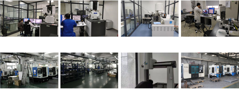
About Us
XKH specializes in high-tech development, production, and sales of special optical glass and new crystal materials. Our products serve optical electronics, consumer electronics, and the military. We offer Sapphire optical components, mobile phone lens covers, Ceramics, LT, Silicon Carbide SIC, Quartz, and semiconductor crystal wafers. With skilled expertise and cutting-edge equipment, we excel in non-standard product processing, aiming to be a leading optoelectronic materials high-tech enterprise.