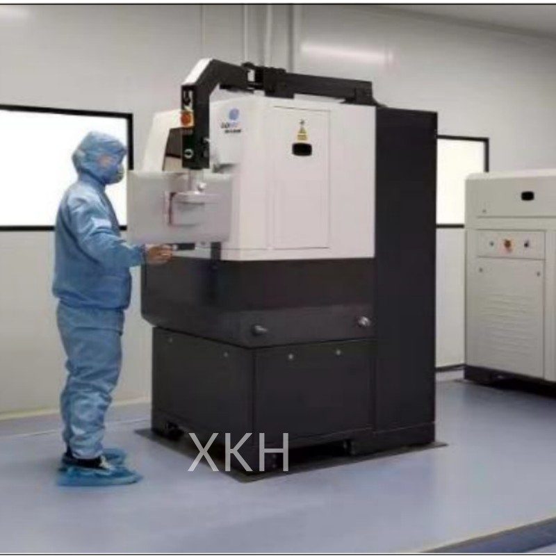
Microjet Water-Guided Laser Cutting System for Advanced Materials


Top Advantages
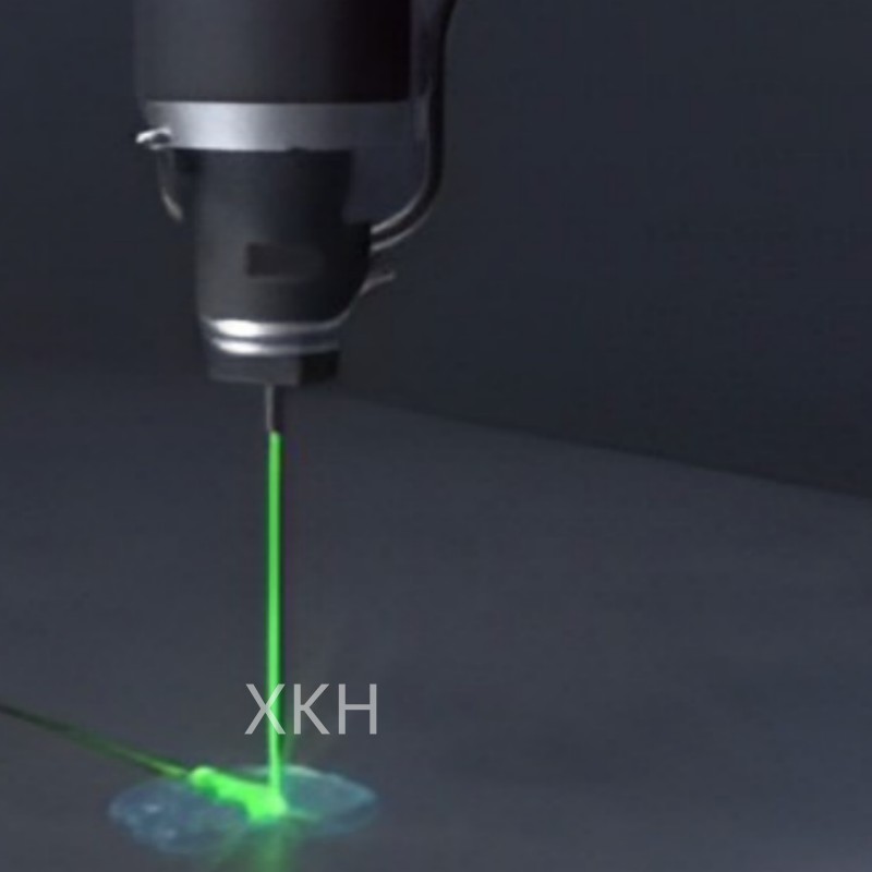
1. Unparalleled Energy Focus through Water Guidance
By using a finely pressurized water jet as a laser waveguide, the system eliminates air interference and ensures full laser focus. The result is ultra-narrow cut widths—as small as 20μm—with sharp, clean edges.
2. Minimal Thermal Footprint
The system’s real-time thermal regulation ensures the heat-affected zone never exceeds 5μm, crucial for preserving material performance and avoiding microcracks.
3. Wide Material Compatibility
Dual-wavelength output (532nm/1064nm) provides enhanced absorption tuning, making the machine adaptable to a variety of substrates, from optically transparent crystals to opaque ceramics.
4. High-Speed, High-Precision Motion Control
With options for linear and direct-drive motors, the system supports high-throughput needs without compromising accuracy. Five-axis motion further enables complex pattern generation and multi-directional cuts.
5. Modular and Scalable Design
Users can tailor system configurations based on application demands—from lab-based prototyping to production-scale deployments—making it suitable across R&D and industrial domains.
Application Areas
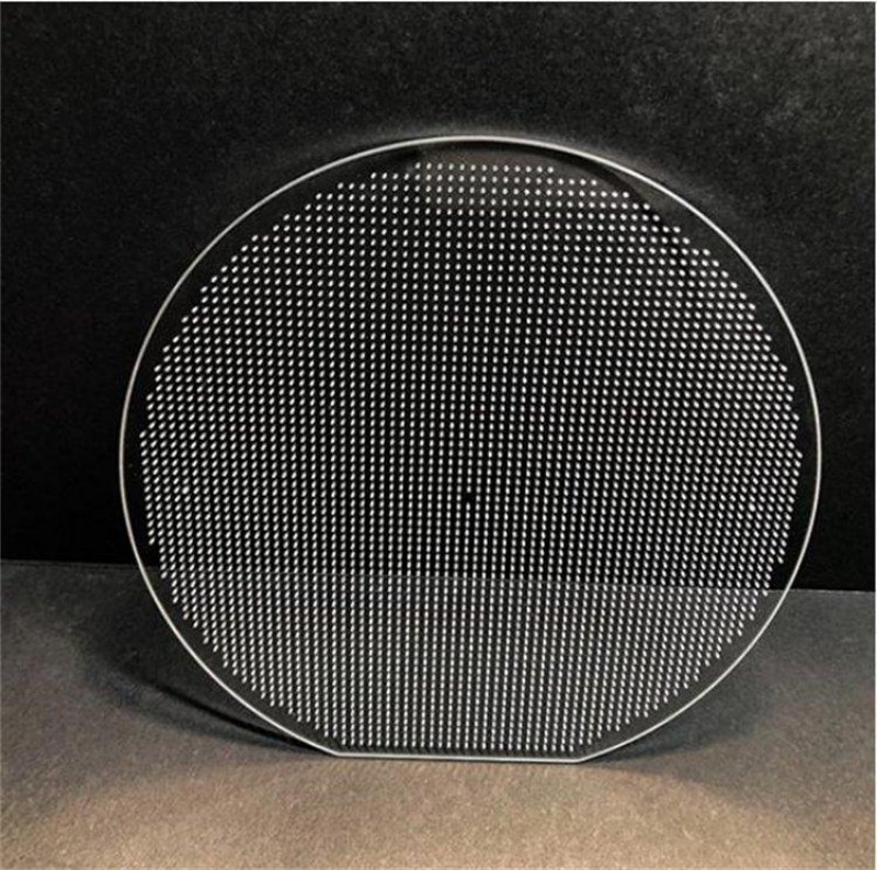
Third-Generation Semiconductors:
Perfect for SiC and GaN wafers, the system performs dicing, trenching, and slicing with exceptional edge integrity.
Diamond and Oxide Semiconductor Machining:
Used for cutting and drilling high-hardness materials like single-crystal diamond and Ga₂O₃, with no carbonization or thermal deformation.
Advanced Aerospace Components:
Supports structural shaping of high-tensile ceramic composites and superalloys for jet engine and satellite components.
Photovoltaic and Ceramic Substrates:
Enables burr-free cutting of thin wafers and LTCC substrates, including through-holes and slot milling for interconnects.
Scintillators and Optical Components:
Maintains surface smoothness and transmission in fragile optical materials like Ce:YAG, LSO, and others.
Specification
|
Feature |
Specification |
| Laser Source | DPSS Nd:YAG |
| Wavelength Options | 532nm / 1064nm |
| Power Levels | 50 / 100 / 200 Watts |
| Precision | ±5μm |
| Cut Width | As narrow as 20μm |
| Heat Affected Zone | ≤5μm |
| Motion Type | Linear / Direct Drive |
| Supported Materials | SiC, GaN, Diamond, Ga₂O₃, etc. |
Why Choose This System?
● Eliminates typical laser machining issues like thermal cracking and edge chipping
● Improves yield and consistency for high-cost materials
● Adaptable for both pilot-scale and industrial use
● Future-proof platform for evolving materials science
Q&A
Q1: What materials can this system process?
A: The system is specially designed for hard and brittle high-value materials. It can effectively process silicon carbide (SiC), gallium nitride (GaN), diamond, gallium oxide (Ga₂O₃), LTCC substrates, aerospace composites, photovoltaic wafers, and scintillator crystals such as Ce:YAG or LSO.
Q2: How does the water-guided laser technology work?
A: It uses a high-pressure microjet of water to guide the laser beam via total internal reflection, effectively channeling laser energy with minimal scattering. This ensures ultra-fine focus, low thermal load, and precision cuts with line widths down to 20μm.
Q3: What are the available laser power configurations?
A: Customers can choose from 50W, 100W, and 200W laser power options depending on their processing speed and resolution needs. All options maintain high beam stability and repeatability.
Detailed Diagram
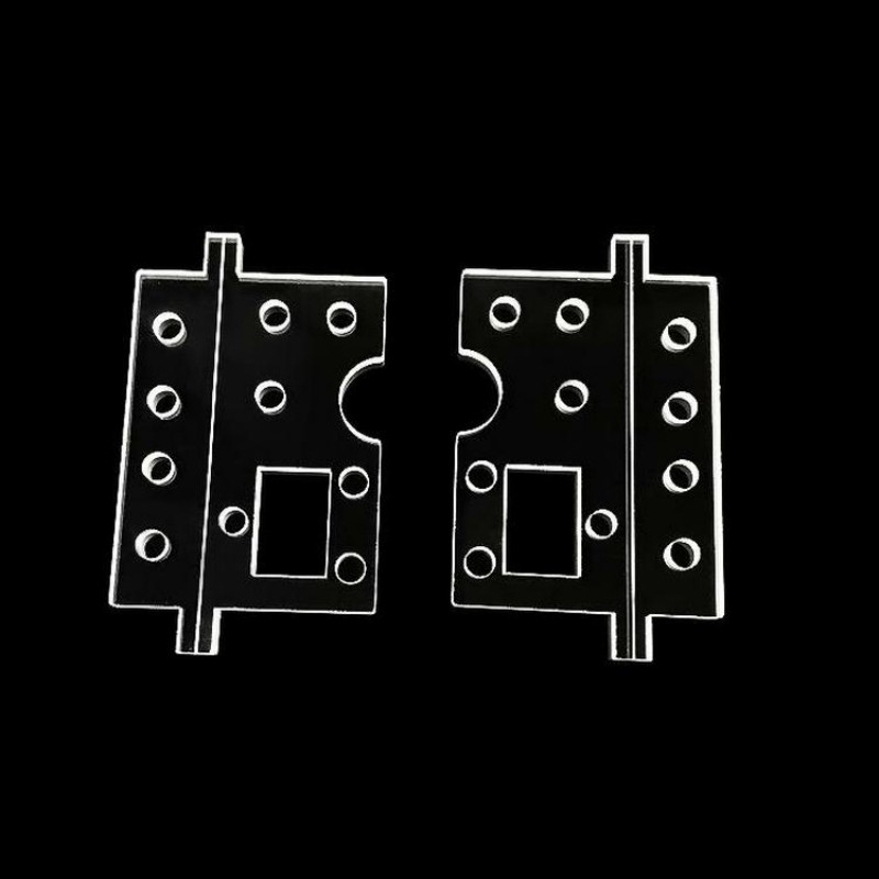
Related Products
-

EFG Sapphire Tube Element Free Galerkin Method
-

Multi-Wire Diamond Sawing Machine for SiC Sapph...
-

Wire Saw Equipment for Sapphire/Ceramics/Marb...
-

3inch Dia76.2mm SiC substrates HPSI Prime Resea...
-

Single Crystal Ruby Rod for Medicine, industry,...
-

6 Inch / 8 Inch POD / FOSB Fiber Optic Splice B...