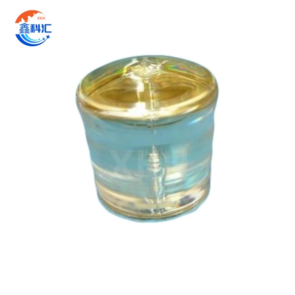
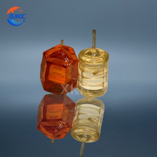
LiTaO3 Lithium Tantalate Ingots with Fe/Mg Doping Customized 4inch 6inch 8inch for Industrial Sensing


Technical parameters
Specification |
Conventional |
High Precision |
Materials |
LiTaO3(LT)/ LiNbO3 wafers |
LiTaO3(LT)/LiNbO3 wafers |
Orientation |
X-112°Y,36°Y,42°Y±0.5° |
X-112°Y,36°Y,42°Y±0.5° |
Parallel |
30″ |
10'' |
Perpendicular |
10′ |
5' |
surface Quality |
40/20 |
20/10 |
Wavefront Distortion |
λ/4@632nm |
λ/8@632nm |
Surface Flatness |
λ/4@632nm |
λ/8@632nm |
Clear Aperture |
>90% |
>90% |
Chamfer |
<0.2×45° |
<0.2×45° |
Thickness/Diameter Tolerance |
±0.1 mm |
±0.1 mm |
Maximum dimensions |
dia150×50mm |
dia150×50mm |
XKH Services
1. Large-Scale Ingot Fabrication
Size and Cutting: 3–8-inch ingots with X/Y/Z-cut, 42°Y-cut, and custom angular cuts (±0.01° tolerance).
Doping Control: Fe/Mg co-doping via Czochralski method (concentration range 10¹⁶–10¹⁹ cm⁻³) to optimize photorefractive resistance and thermal stability.
2. Advanced Process Technologies
Heterogeneous Integration: Silicon-based LiTaO3 composite wafers (POI) with thickness control (300–600 nm) and thermal conductivity up to 8.78 W/m·K for high-frequency SAW filters.
Waveguide Fabrication: Proton exchange (PE) and reverse proton exchange (RPE) techniques, achieving submicron waveguides (Δn >0.7) for high-speed electro-optic modulators (bandwidth >40 GHz).
3. Quality Management Systems
End-to-End Testing: Raman spectroscopy (polytype verification), XRD (crystallinity), AFM (surface morphology), and optical uniformity testing (Δn <5×10⁻⁵).
4. Global Supply Chain Support
Production Capacity: Monthly output >5,000 ingots (8-inch: 70%), supporting 48-hour emergency delivery.
Logistics Network: Coverage in Europe, North America, and Asia-Pacific via air/sea freight with temperature-controlled packaging.
5. Technical Co-Development
Joint R&D Labs: Collaborate on photonic integration platforms (e.g., SiO2 low-loss layer bonding).
Summary
LiTaO3 Ingots serve as strategic materials reshaping optoelectronics and quantum technologies. Through innovations in crystal growth (e.g., PVT), defect mitigation, and heterogeneous integration (e.g., POI), we deliver high-reliability, cost-effective solutions for 5G/6G communications, quantum computing, and industrial IoT. XKH commitment to advancing ingot defect reduction and scaling 8-inch production ensures clients lead in global supply chains, driving the next era of wide-bandgap semiconductor ecosystems.