CVD SiC Components for Semiconductor Equipment SiC Ring SiC Electrode Dry Etch


Detailed Diagram


For Semiconductor Equipment Applications
CVD SiC components are key consumable and structural parts used in semiconductor front-end equipment. They are widely applied in Dry Etch, EPI, Diffusion, and RTP processes.
With excellent high purity, thermal conductivity, plasma corrosion resistance, high-temperature stability, low particle generation, and precision machinability, CVD SiC components are suitable for demanding semiconductor process environments.
Dry Etch Application
In dry etching equipment, CVD SiC and silicon components are mainly installed inside the process chamber. They are used for plasma control, wafer edge protection, electrode systems, chamber protection, and process uniformity improvement.
Typical Components
| Component | Material | Application |
|---|---|---|
| Inner Electrode | Si / SiC | Used in the electrode system to control plasma reaction |
| Outer Electrode | Si / SiC | Works with the inner electrode to improve etching uniformity |
| C-Shroud Ring | Si | Used for chamber protection and plasma/gas flow control |
| Hot Edge Ring | Si / SiC | Protects wafer edges and improves edge etching performance |
| Ground Cover Ring | Quartz | Used for grounding and chamber protection |
| Couple Ring | Quartz | Supporting and coupling component inside the chamber |
| Quartz Ring | Quartz | Used for sealing, support, or insulation in the chamber |
Key Advantages
CVD SiC components offer excellent resistance to plasma corrosion in fluorine-based and chlorine-based etching environments. They help reduce particle contamination, minimize component wear, extend maintenance intervals, and improve process stability.

Main Product Series
Si Electrode
Si Electrodes are mainly used in dry etching equipment as electrode components. They are suitable for mature semiconductor processes and equipment spare part replacement.
| Item | Specification |
|---|---|
| Material | Single Crystal Silicon |
| Max Diameter | Max 480 mm |
| Resistivity | Low Res. <0.02 Ω·cm; Middle Res. 1–4 Ω·cm; High Res. 70–90 Ω·cm |
| RRG | <5% |
| Gas Hole | Diameter 0.2–0.8 mm |
| Surface Condition | Polished / Lapped / Ground |
| Machining Precision | <10 μm |
| Quality Inspection | Free of chips, scratches, cracks, stains and other defects |

Si Ring
Si Rings are used in etching chambers for wafer edge protection, support, and plasma control.
| Item | Specification |
|---|---|
| Material | Single Crystal Silicon / Multi Crystal Silicon |
| Max Diameter | Max 480 mm |
| Resistivity | Low Res. <0.02 Ω·cm; Middle Res. 1–4 Ω·cm; High Res. 70–90 Ω·cm |
| RRG | <5% |
| Surface Condition | Polished / Lapped / Ground |
| Machining Precision | <10 μm |
| Quality Inspection | Free of chips, scratches, cracks, stains and other defects |
CVD SiC Ring
CVD SiC Rings are used as edge rings, protection rings, and support rings in Dry Etch, EPI, RTP, and other semiconductor equipment.
| Item | Specification |
|---|---|
| Material | CVD SiC |
| Max Diameter | Max 370 mm |
| Resistivity | Low Res. <0.02 Ω·cm; Middle Res. 0.2–25 Ω·cm; High Res. >100 Ω·cm |
| RRG | <5% |
| Surface Condition | Ground |
| Machining Precision | <10 μm |
| Quality Inspection | Free of chips, scratches, cracks, stains and other defects |
CVD SiC Electrode
CVD SiC Electrodes are used as key electrode components in dry etching equipment. Compared with conventional silicon electrodes, CVD SiC electrodes provide better corrosion resistance and longer service life.
| Item | Specification |
|---|---|
| Material | CVD SiC |
| Max Diameter | Max 330 mm |
| Resistivity | Low Res. <0.02 Ω·cm; Middle Res. 0.2–25 Ω·cm; High Res. >100 Ω·cm |
| RRG | <5% |
| Surface Condition | Ground |
| Machining Precision | <10 μm |
| Quality Inspection | Free of chips, scratches, cracks, stains and other defects |

Material Properties of CVD Polycrystalline SiC
CVD polycrystalline SiC is produced by chemical vapor deposition. It features a dense structure, high purity, excellent corrosion resistance, and strong stability in semiconductor clean process environments.
| Property | Unit | Typical Value |
|---|---|---|
| Density | g/cm³ | 3.21–3.22 |
| Flexural Strength | MPa | 320–380 |
| Thermal Conductivity | W/m·K | 240–360 |
| Grain Size | μm | 5–10 |
| Purity | % | 99.99997 |
| Vickers Microhardness | HV | 3100–3700 |
| Elastic Modulus | GPa | 450–530 |
| XRD Rate | - | 0.65–1.1 |
| CTE, RT to 1000°C | 10⁻⁶/K | 4.8–5.1 |

FAQ
Q1: What are CVD polycrystalline SiC components used for?
CVD polycrystalline SiC components are mainly used in semiconductor front-end equipment, includingDry Etch, EPI, Diffusion, and RTP systems. Typical products include SiC rings, SiC electrodes, edge rings, susceptors, SiC boats, and dummy wafers.
Q2: What are the advantages of CVD SiC compared with quartz or silicon parts?
CVD SiC offers better plasma corrosion resistance, high-temperature stability, thermal conductivity, hardness, and service life. It can reduceparticle generation and component wear in harsh semiconductor processenvironments.
Q3: What materials are available for these components?
We can provide components made from CVD SiC, single crystal silicon, multi-crystal silicon, and quartz, depending on the application and equipmentrequirements.
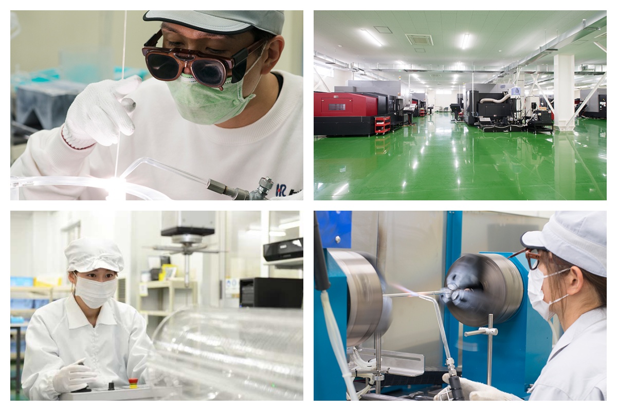
About Us
XKH specializes in high-tech development, production, and sales of special optical glass and new crystal materials. Our products serve optical electronics, consumer electronics, and the military. We offer Sapphire optical components, mobile phone lens covers, Ceramics, LT, Silicon Carbide SIC, Quartz, and semiconductor crystal wafers. With skilled expertise and cutting-edge equipment, we excel in non-standard product processing, aiming to be a leading optoelectronic materials high-tech enterprise.