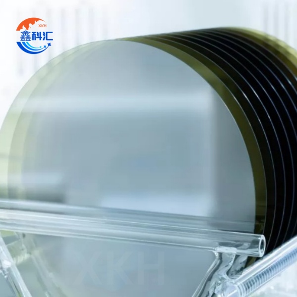
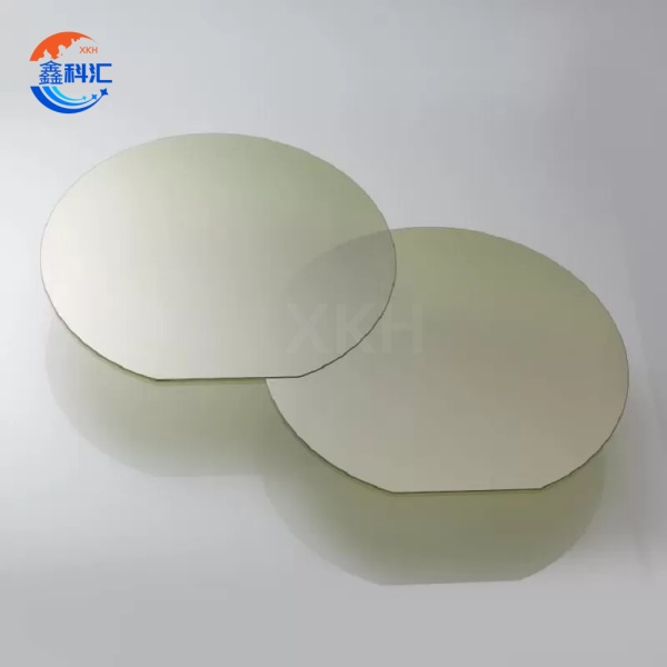
12 inch SiC Substrate N Type Large Size High Performance RF Applications


Technical parameters
| 12 inch Silicon Carbide (SiC) Substrate Specification | |||||
| Grade | ZeroMPD Production Grade(Z Grade) |
Standard Production Grade(P Grade) |
Dummy Grade (D Grade) |
||
| Diameter | 3 0 0 mm~1305mm | ||||
| Thickness | 4H-N | 750μm±15 μm | 750μm±25 μm | ||
| 4H-SI | 750μm±15 μm | 750μm±25 μm | |||
| Wafer Orientation | Off axis : 4.0° toward <1120 >±0.5° for 4H-N, On axis : <0001>±0.5° for 4H-SI | ||||
| Micropipe Density | 4H-N | ≤0.4cm-2 | ≤4cm-2 | ≤25cm-2 | |
| 4H-SI | ≤5cm-2 | ≤10cm-2 | ≤25cm-2 | ||
| Resistivity | 4H-N | 0.015~0.024 Ω·cm | 0.015~0.028 Ω·cm | ||
| 4H-SI | ≥1E10 Ω·cm | ≥1E5 Ω·cm | |||
| Primary Flat Orientation | {10-10} ±5.0° | ||||
| Primary Flat Length | 4H-N | N/A | |||
| 4H-SI | Notch | ||||
| Edge Exclusion | 3 mm | ||||
| LTV/TTV/Bow /Warp | ≤5μm/≤15μm/≤35 μm/≤55 μm | ≤5μm/≤15μm/≤35 □ μm/≤55 □ μm | |||
| Roughness | Polish Ra≤1 nm | ||||
| CMP Ra≤0.2 nm | Ra≤0.5 nm | ||||
| Edge Cracks By High Intensity Light Hex Plates By High Intensity Light Polytype Areas By High Intensity Light Visual Carbon Inclusions Silicon Surface Scratches By High Intensity Light |
None Cumulative area ≤0.05% None Cumulative area ≤0.05% None |
Cumulative length ≤ 20 mm, single length≤2 mm Cumulative area ≤0.1% Cumulative area≤3% Cumulative area ≤3% Cumulative length≤1×wafer diameter |
|||
| Edge Chips By High Intensity Light | None permitted ≥0.2mm width and depth | 7 allowed, ≤1 mm each | |||
| (TSD) Threading screw dislocation | ≤500 cm-2 | N/A | |||
| (BPD) Base plane dislocation | ≤1000 cm-2 | N/A | |||
| Silicon Surface Contamination By High Intensity Light | None | ||||
| Packaging | Multi-wafer Cassette Or Single Wafer Container | ||||
| Notes: | |||||
| 1 Defects limits apply to entire wafer surface except for the edge exclusion area. 2The scratches should be checked on Si face only. 3 The dislocation data is only from KOH etched wafers. |
|||||
Key Features
1. Large Size Advantage: The 12-inch SiC substrate (12-inch silicon carbide substrate) offers a larger single-wafer area, enabling more chips to be produced per wafer, thereby reducing manufacturing costs and increasing yield.
2. High-Performance Material: Silicon carbide’s high-temperature resistance and high breakdown field strength make the 12-inch substrate ideal for high-voltage and high-frequency applications, such as EV inverters and fast-charging systems.
3. Processing Compatibility: Despite the high hardness and processing challenges of SiC, the 12-inch SiC substrate achieves lower surface defects through optimized cutting and polishing techniques, improving device yield.
4. Superior Thermal Management: With better thermal conductivity than silicon-based materials, the 12-inch substrate effectively addresses heat dissipation in high-power devices, extending equipment lifespan.
Main Applications
1. Electric Vehicles: The 12-inch SiC substrate (12-inch silicon carbide substrate) is a core component of next-generation electric drive systems, enabling high-efficiency inverters that enhance range and reduce charging time.
2. 5G Base Stations: Large-size SiC substrates support high-frequency RF devices, meeting the demands of 5G base stations for high power and low loss.
3.Industrial Power Supplies: In solar inverters and smart grids, the 12-inch substrate can withstand higher voltages while minimizing energy loss.
4.Consumer Electronics: Future fast chargers and data center power supplies may adopt 12-inch SiC substrates to achieve compact size and higher efficiency.
XKH's Services
We specialize in customized processing services for 12-inch SiC substrates (12-inch silicon carbide substrates), including:
1. Dicing & Polishing: Low-damage, high-flatness substrate processing tailored to customer requirements, ensuring stable device performance.
2. Epitaxial Growth Support: High-quality epitaxial wafer services to accelerate chip manufacturing.
3. Small-Batch Prototyping: Supports R&D validation for research institutions and enterprises, shortening development cycles.
4. Technical Consulting: End-to-end solutions from material selection to process optimization, helping customers overcome SiC processing challenges.
Whether for mass production or specialized customization, our 12-inch SiC substrate services align with your project needs, empowering technological advancements.
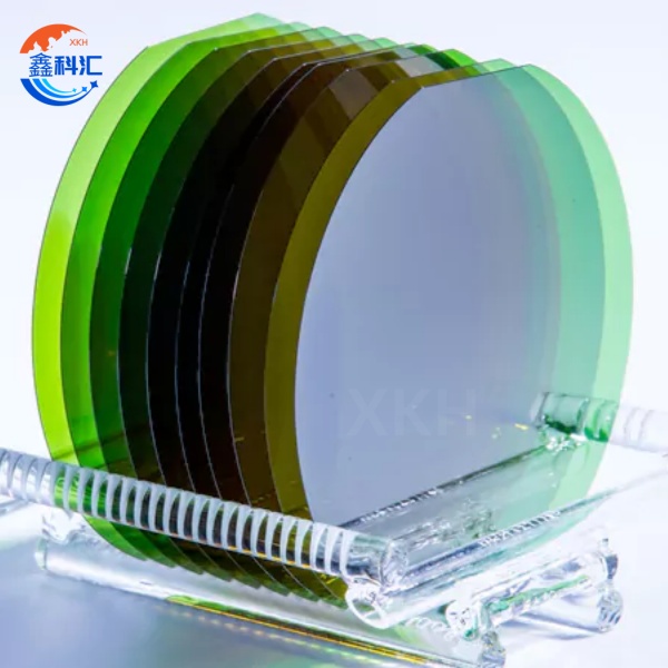
Related Products
-
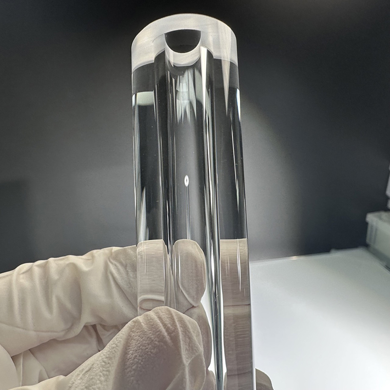
Transparent sapphire tubes pipes rods high temp...
-

Ruby optics Ruby rod optical window titanium ge...
-

AlN-on-NPSS Wafer: High-Performance Aluminum Ni...
-

Purple color violet sapphire Al2O3 material for...
-

Silicon / Silicon Carbide (SiC) Wafer Four-Stag...
-

LiNbO₃ Wafers 2inch-8inch Thickness 0.1 ~ 0.5mm...