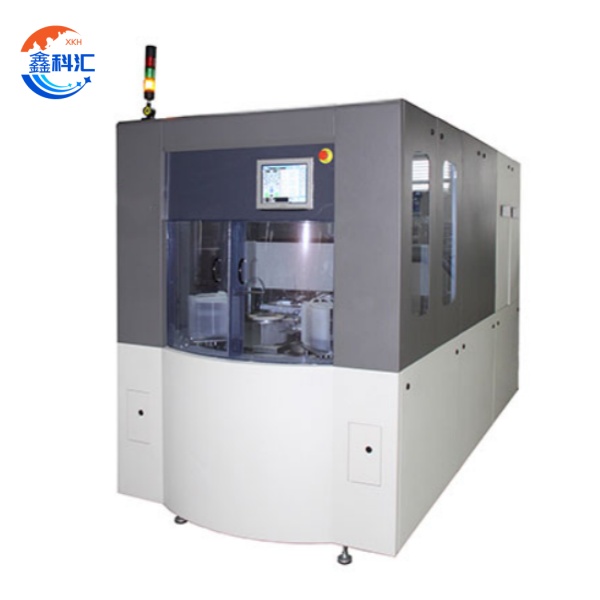
Wafer Thinning Equipment for 4 Inch-12 Inch Sapphire/SiC/Si Wafers Processing


Working Principle
The wafer thinning process operates through three stages:
Rough Grinding: A diamond wheel (grit size 200–500 μm) removes 50–150 μm of material at 3000–5000 rpm to rapidly reduce thickness.
Fine Grinding: A finer wheel (grit size 1–50 μm) reduces thickness to 20–50 μm at <1 μm/s to minimize subsurface damage.
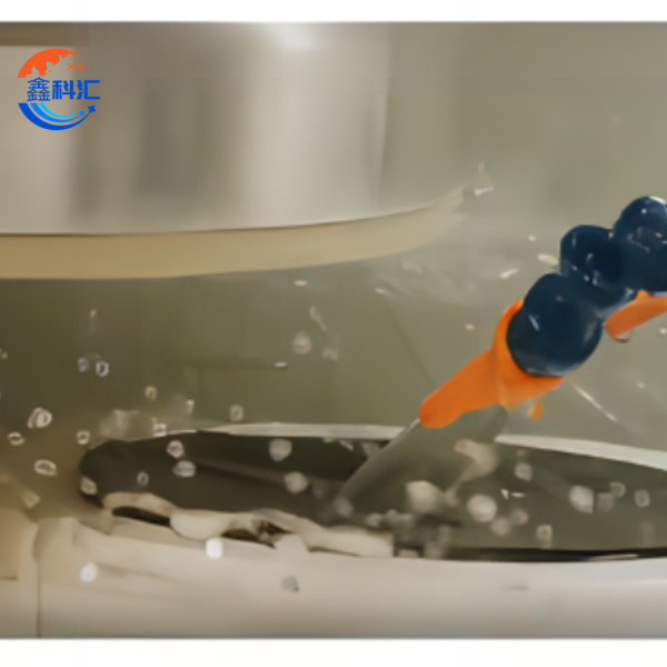
Polishing (CMP): A chemical-mechanical slurry eliminates residual damage, achieving Ra <0.1 nm.
Compatible Materials
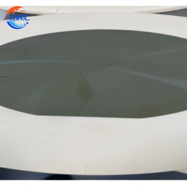
Silicon (Si): Standard for CMOS wafers, thinned to 25 μm for 3D stacking.
Silicon Carbide (SiC): Requires specialized diamond wheels (80% diamond concentration) for thermal stability.
Sapphire (Al₂O₃): Thinned to 50 μm for UV LED applications.
Core System Components
1. Grinding System
Dual-Axis Grinder: Combines coarse/fine grinding in a single platform, reducing cycle time by 40%.
Aerostatic Spindle: 0–6000 rpm speed range with <0.5 μm radial runout.
2. Wafer Handling System
Vacuum Chuck: >50 N holding force with ±0.1 μm positioning accuracy.
Robotic Arm: Transports 4–12-inch wafers at 100 mm/s.
3. Control System
Laser Interferometry: Real-time thickness monitoring (resolution 0.01 μm).
AI-Driven Feedforward: Predicts wheel wear and adjusts parameters automatically.
4. Cooling & Cleaning
Ultrasonic Cleaning: Removes particles >0.5 μm with 99.9% efficiency.
Deionized Water: Cools wafer to <5°C above ambient.
Core Advantages
1. Ultra-High Precision: TTV (Total Thickness Variation) <0.5 μm, WTW (Within-Wafer Thickness Variation) <1 μm.
2. Multi-Process Integration: Combines grinding, CMP, and plasma etching in one machine.
3. Material Compatibility:
Silicon: Thickness reduction from 775 μm to 25 μm.
SiC: Achieves <2 μm TTV for RF applications.
Doped Wafers: Phosphorus-doped InP wafers with <5% resistivity drift.
4. Smart Automation: MES integration reduces human error by 70%.
5. Energy Efficiency: 30% lower power consumption via regenerative braking.
Key Applications
1. Advanced Packaging
• 3D ICs: Wafer thinning enables vertical stacking of logic/memory chips (e.g., HBM stacks), achieving 10× higher bandwidth and 50% reduced power consumptioncompared to 2.5D solutions. The equipment supports hybrid bonding and TSV (Through-Silicon Via) integration, critical for AI/ML processors requiring <10 μm interconnect pitch. For example, 12-inch wafers thinned to 25 μm allow stacking 8+ layers while maintaining <1.5% warpage, essential for automotive LiDAR systems.
• Fan-Out Packaging: By reducing wafer thickness to 30 μm, interconnect length is shortened by 50%, minimizing signal delay (<0.2 ps/mm) and enabling 0.4 mm ultra-thin chiplets for mobile SoCs. The process leverages stress-compensated grinding algorithms to prevent warpage (>50 μm TTV control), ensuring reliability in high-frequency RF applications.
2. Power Electronics
• IGBT Modules: Thinning to 50 μm reduces thermal resistance to <0.5°C/W, enabling 1200V SiC MOSFETs to operate at 200°C junction temperatures. Our equipment employs multi-stage grinding (coarse: 46 μm grit → fine: 4 μm grit) to eliminate subsurface damage, achieving >10,000 cycles of thermal cycling reliability. This is critical for EV inverters, where 10 μm-thick SiC wafers improve switching speed by 30% .
• GaN-on-SiC Power Devices: Wafer thinning to 80 μm enhances electron mobility (μ > 2000 cm²/V·s) for 650V GaN HEMTs, reducing conduction losses by 18%. The process uses laser-assisted dicing to prevent cracking during thinning, achieving <5 μm edge chipping for RF power amplifiers.
3. Optoelectronics
• GaN-on-SiC LEDs: 50 μm sapphire substrates improve light extraction efficiency (LEE) to 85% (vs. 65% for 150 μm wafers) by minimizing photon trapping. Our equipment’s ultra-low TTV control (<0.3 μm) ensures uniform LED emission across 12-inch wafers, critical for Micro-LED displaysrequiring <100nm wavelength uniformity.
• Silicon Photonics: 25μm-thick silicon wafers enable 3 dB/cm lower propagation loss in waveguides, essential for 1.6 Tbps optical transceivers. The process integrates CMP smoothing to reduce surface roughness to Ra <0.1 nm, enhancing coupling efficiency by 40% .
4. MEMS Sensors
• Accelerometers: 25 μm silicon wafers achieve SNR >85 dB (vs. 75 dB for 50 μm wafers) by increasing proof-mass displacement sensitivity. Our dual-axis grindingsystem compensates for stress gradients, ensuring <0.5% sensitivity drift over -40°C to 125°C. Applications include automotive crash detection and AR/VR motion tracking.
• Pressure Sensors: Thinning to 40 μm enables0–300 bar measurement rangeswith <0.1% FS hysteresis. Using temporary bonding (glass carriers), the process avoids wafer fracture during backside etching, achieving <1 μm overpressure tolerance for industrial IoT sensors.
• Technical Synergy: Our wafer thinning equipment unifies mechanical grinding, CMP, and plasma etching to address diverse material challenges (Si, SiC, Sapphire). For instance, GaN-on-SiC requires hybrid grinding (diamond wheels + plasma) to balance hardness and thermal expansion, while MEMS sensors demand sub-5 nm surface roughness via CMP polishing.
• Industry Impact: By enabling thinner, higher-performance wafers, this technology drives innovations in AI chips, 5G mmWave modules, and flexible electronics, with TTV tolerances <0.1 μm for foldable displays and <0.5 μm for automotive LiDAR sensors.
XKH's Services
1. Customized Solutions
Scalable Configurations: 4–12-inch chamber designs with automated loading/unloading.
Doping Support: Custom recipes for Er/Yb-doped crystals and InP/GaAs wafers.
2. End-to-End Support
Process Development: Free trial runs with optimization.
Global Training: Technical workshops annually on maintenance and troubleshooting.
3. Multi-Material Processing
SiC: Wafer thinning to 100 μm with Ra <0.1 nm.
Sapphire: 50μm thickness for UV laser windows (transmittance >92%@200 nm).
4. Value-Added Services
Consumable Supply: Diamond wheels (2000+ wafers/life) and CMP slurries.
Conclusion
This wafer thinning equipment deliversindustry-leading precision,multi-material versatility,and smart automation, making it indispensable for 3D integration and power electronics. XKH comprehensive services—from customization to post-processing—ensure clients achieve cost efficiency and performance excellence in semiconductor manufacturing.