Wafer Single Carrier Box 1″2″3″4″6″


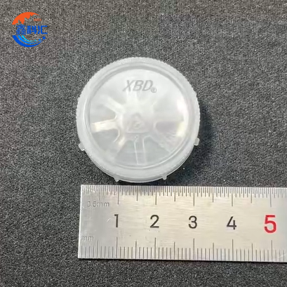
Detailed Diagram


Product Introduction
The Wafer Single Carrier Box is a precision-engineered container designed to hold and protect a single silicon wafer during transportation, storage, or cleanroom handling. These boxes are widely used across the semiconductor, optoelectronic, MEMS, and compound material industries where ultra-clean and anti-static protection is essential for maintaining wafer integrity.
Available in a range of standard sizes—including 1-inch, 2-inch, 3-inch, 4-inch, and 6-inch diameters—our wafer single boxes offer versatile solutions for laboratories, R&D centers, and manufacturing facilities requiring safe, repeatable wafer handling for individual units.
Key Features
-
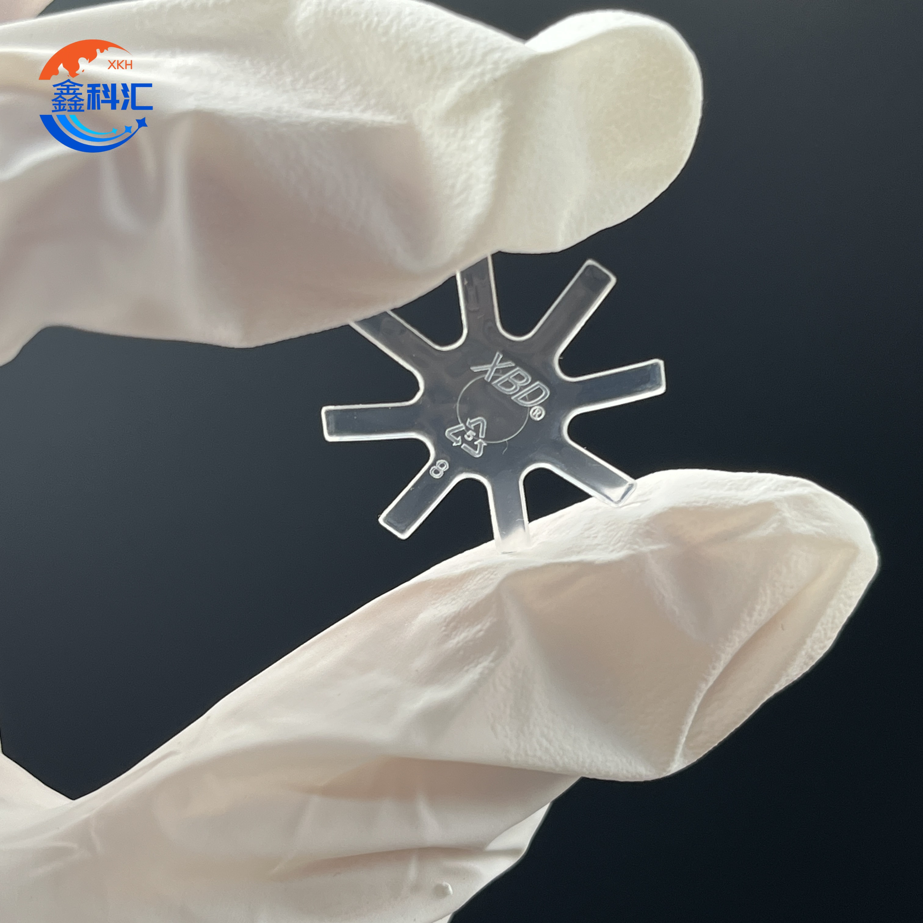
Precise Fit Design: Each box is custom-molded to fit one wafer of a specific size with high precision, ensuring a snug and secure hold that prevents sliding or scratching.
-
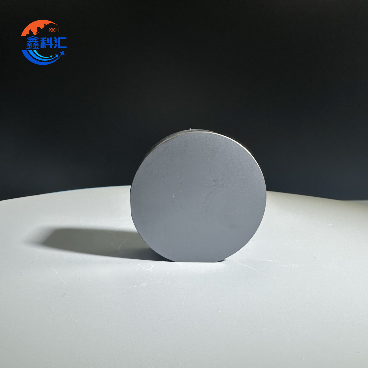
High-Purity Materials: Manufactured from cleanroom-compatible polymers such as Polypropylene (PP), Polycarbonate (PC), or antistatic Polyethylene (PE), offering chemical resistance, durability, and minimal particle generation.
-
Anti-Static Options: Optional conductive and ESD-safe materials help prevent electrostatic discharge during handling.
-
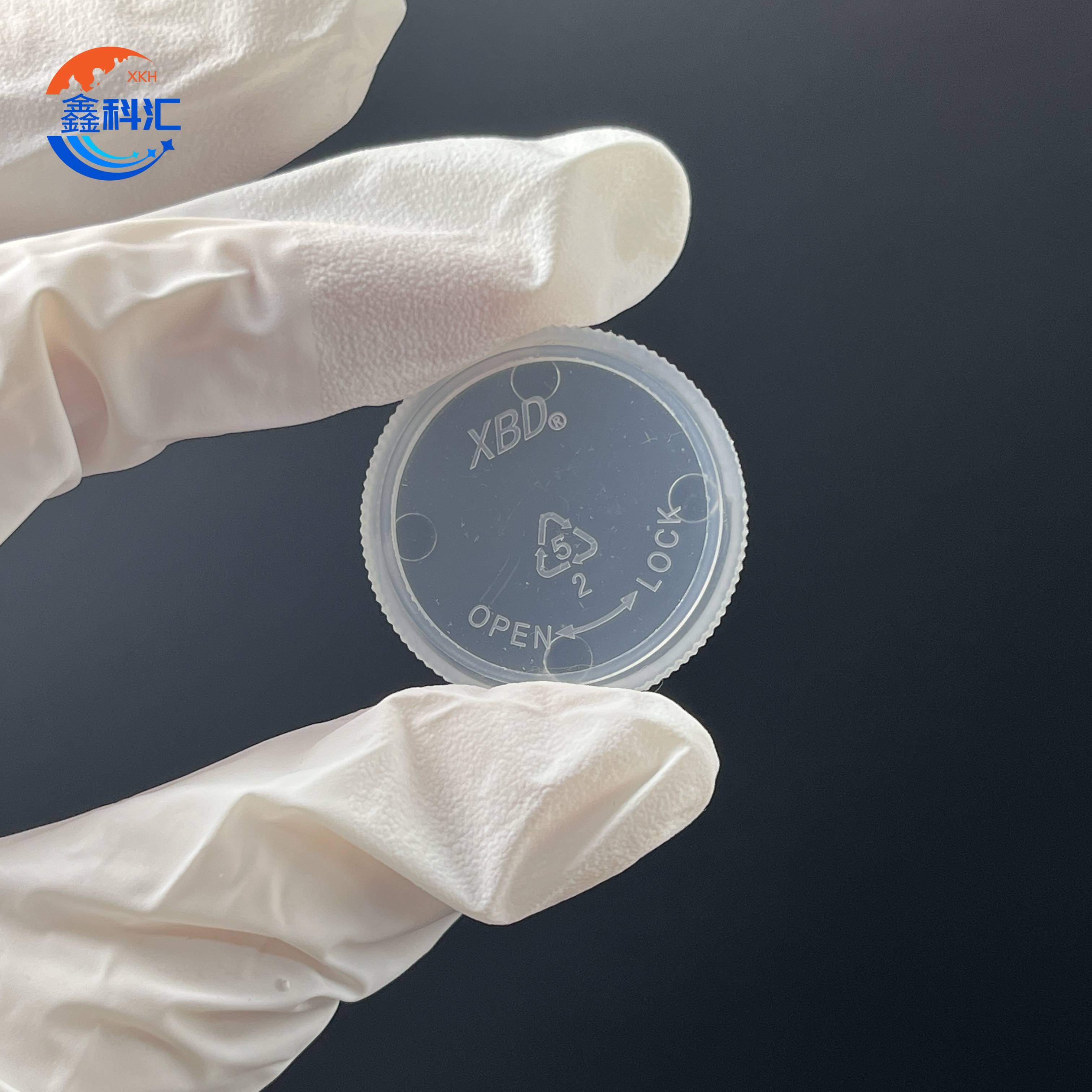
Secure Locking Mechanism: Snap-fit or twist-lock lids provide firm closure and ensure airtight sealing to prevent contamination.
-
Stackable Form Factor: Allows for organized storage and optimized space usage.
Applications
-
Safe transport and storage of individual silicon wafers
-
R&D and QA wafer sampling
-
Compound semiconductor wafer handling (e.g., GaAs, SiC, GaN)
-
Cleanroom packaging for ultra-thin or sensitive wafers
-
Chip-level packaging or post-process wafer delivery

Available Sizes
| Size (Inch) | External Diameter |
|---|---|
| 1" | ~38mm |
| 2" | ~50.8mm |
| 3" | ~76.2mm |
| 4" | ~100mm |
| 6" | ~150mm |

FAQ
Q1: Are these boxes suitable for ultra-thin wafers?
A1: Yes. We provide cushioned or soft-insert versions for wafers under 100µm thickness to prevent edge chipping or warping.
Q2: Can I get a customized logo or labeling?
A2: Absolutely. We support laser engraving, ink printing, and barcode/QR code labeling as per your request.
Q3: Are the boxes reusable?
A3: Yes. They are built from durable and chemically stable materials for repeated usage in cleanroom environments.
Q4: Do you offer vacuum-sealing or nitrogen-sealing support?
A4: While the boxes are not vacuum-sealed by default, we offer add-ons like purge valves or double O-ring seals for special storage requirements.
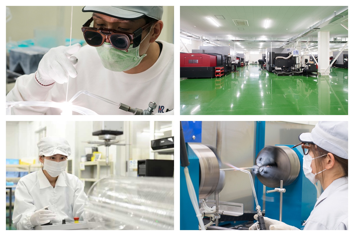
About Us
XKH specializes in high-tech development, production, and sales of special optical glass and new crystal materials. Our products serve optical electronics, consumer electronics, and the military. We offer Sapphire optical components, mobile phone lens covers, Ceramics, LT, Silicon Carbide SIC, Quartz, and semiconductor crystal wafers. With skilled expertise and cutting-edge equipment, we excel in non-standard product processing, aiming to be a leading optoelectronic materials high-tech enterprise.