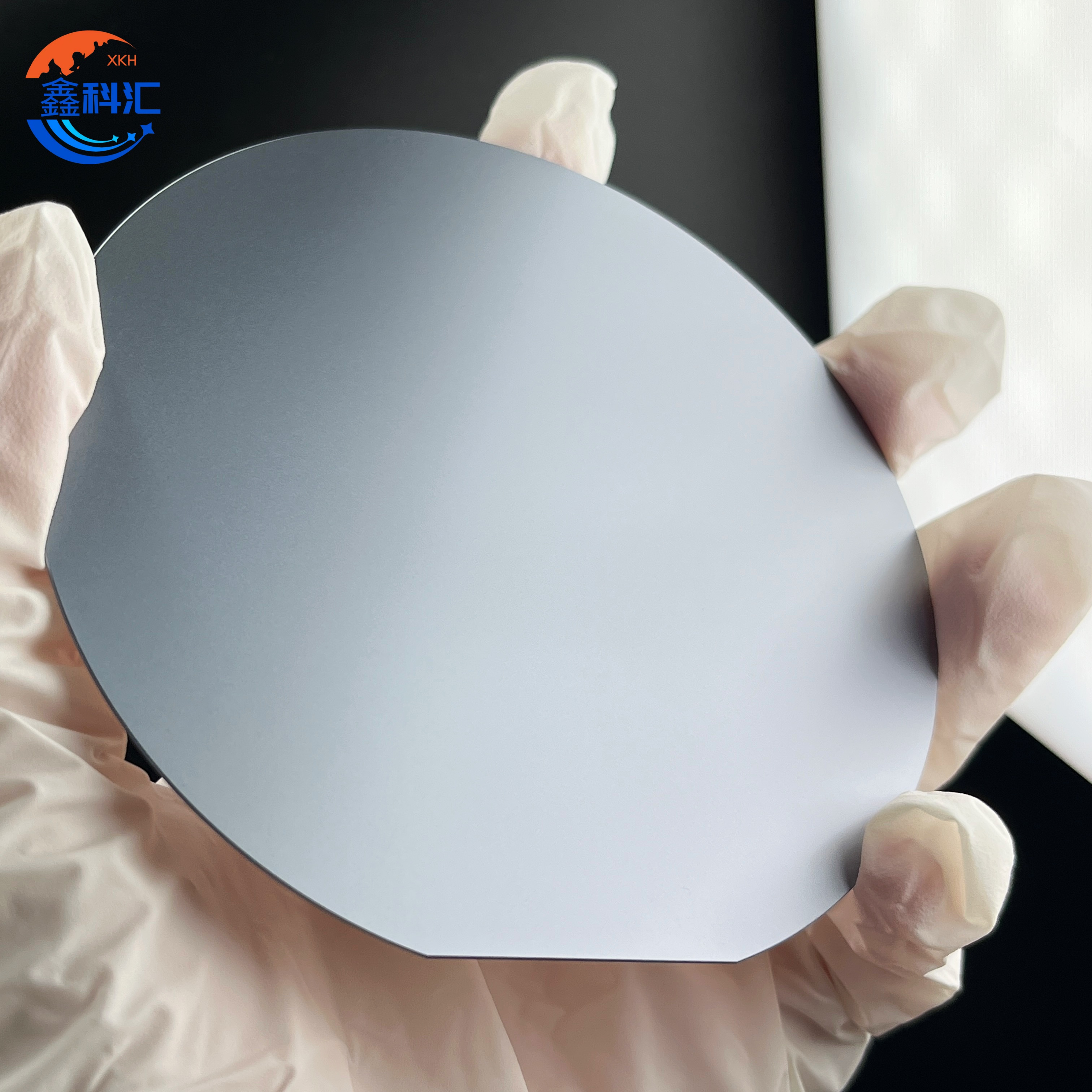
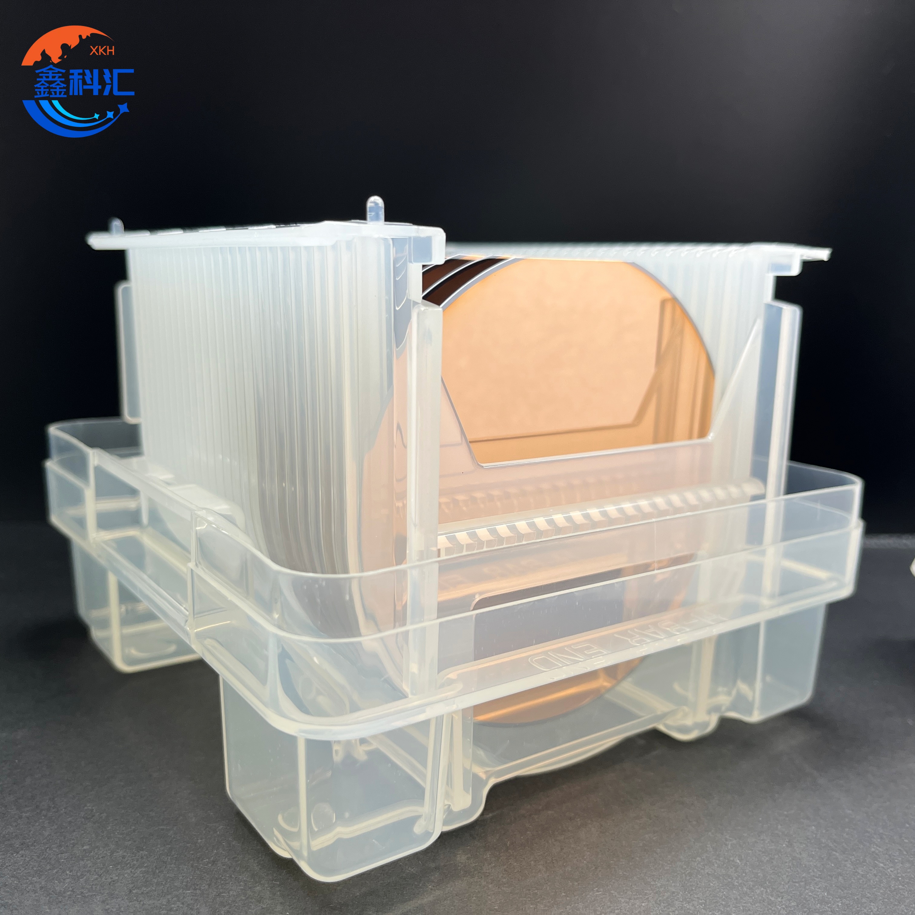
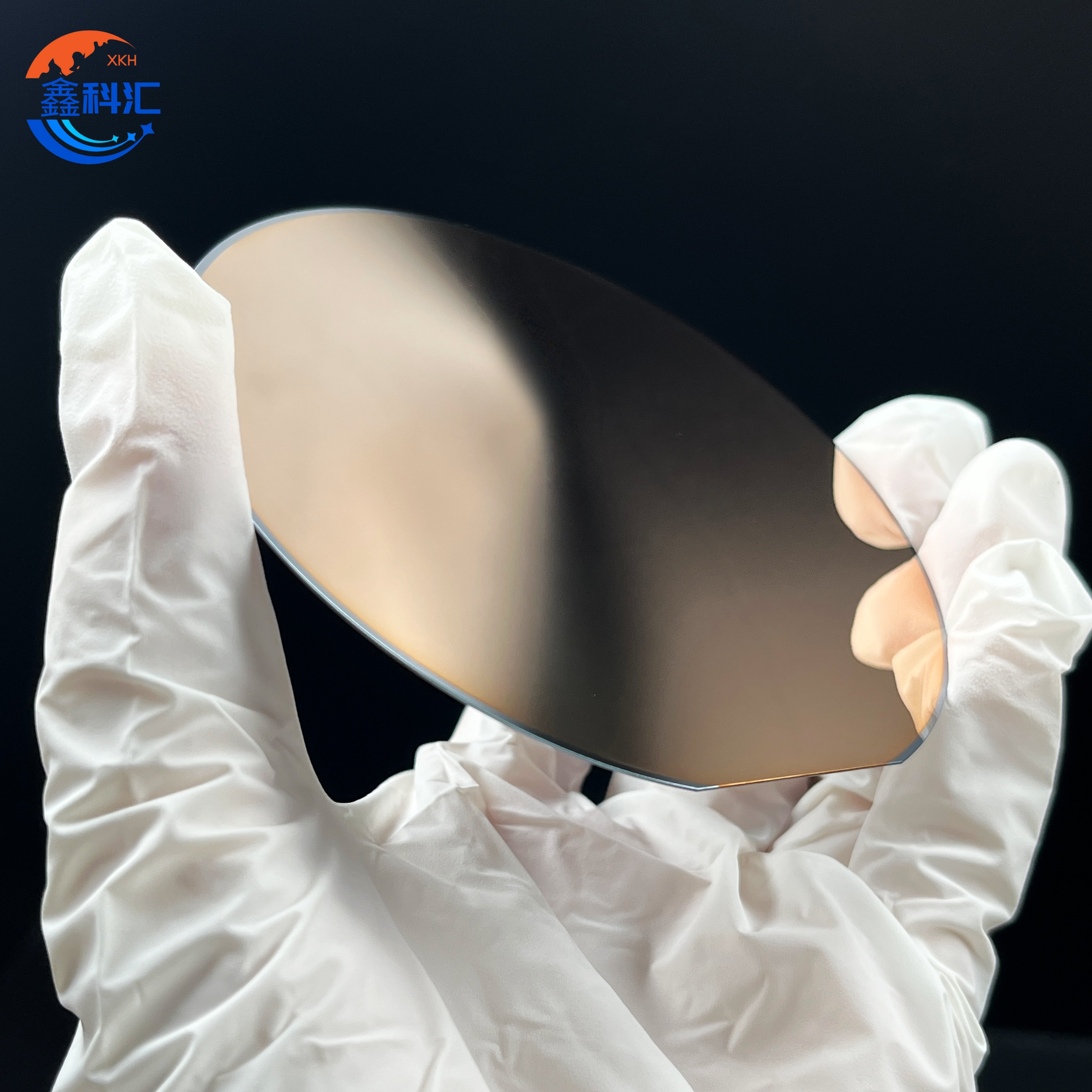
Ti/Cu Metal-Coated Silicon Wafer (Titanium/Copper)


Detailed Diagram


Overview
Our Ti/Cu metal-coated silicon wafers feature a high-quality silicon (or optional glass/quartz) substrate coated with a titanium adhesion layer and a copper conductive layer using standard magnetron sputtering. The Ti interlayer significantly improves adhesion and process stability, while the Cu top layer offers a low-resistance, uniform surface ideal for electrical interfacing and downstream microfabrication.
Designed for both research and pilot-scale applications, these wafers are available in multiple sizes and resistivity ranges, with flexible customization for thickness, substrate type, and coating configuration.
Key Features
-
Strong adhesion & reliability: Ti bonding layer enhances film adherence to Si/SiO₂ and improves handling robustness
-
High conductivity surface: Cu coating provides excellent electrical performance for contacts and test structures
-
Wide customization range: wafer size, resistivity, orientation, substrate thickness, and film thickness available on request
-
Process-ready substrates: compatible with common lab and fab workflows (lithography, electroplating build-up, metrology, etc.)
-
Material series available: besides Ti/Cu, we also offer Au, Pt, Al, Ni, Ag metal-coated wafers
Typical Structure & Deposition
-
Stack: Substrate + Ti adhesion layer + Cu coating layer
-
Standard process: Magnetron sputtering
-
Optional processes: Thermal evaporation / Electroplating (for thicker Cu requirements)
Mechanical Properties of Quartz Glass
| Item | Options |
|---|---|
| Wafer size | 2", 4", 6", 8"; 10×10 mm; custom dicing sizes |
| Conductivity type | P-type / N-type / Intrinsic high-resistivity (Un) |
| Orientation | <100>, <111>, etc. |
| Resistivity | <0.0015 Ω·cm; 1–10 Ω·cm; >1000–10000 Ω·cm |
| Thickness (µm) | 2": 200/280/400/500; 4": 450/500/525; 6": 625/650/675; 8": 650/700/725/775; custom |
| Substrate materials | Silicon; optional quartz, BF33 glass, etc. |
| Film thickness | 10 nm / 50 nm / 100 nm / 150 nm / 300 nm / 500 nm / 1 µm (customizable) |
| Metal film options | Ti/Cu; also Au, Pt, Al, Ni, Ag available |

Applications
-
Ohmic contact & conductive substrates for device R&D and electrical testing
-
Seed layers for electroplating (RDL, MEMS structures, thick Cu build-up)
-
Sol–gel and nanomaterial growth substrates for nano and thin-film research
-
Microscopy & surface metrology (SEM/AFM/SPM sample prep and measurement)
-
Bio/chemical surfaces such as cell culture platforms, protein/DNA microarrays, and reflectometry substrates
FAQ (Ti/Cu Metal-Coated Silicon Wafers)
Q1: Why is a Ti layer used under the Cu coating?
A: Titanium works as an adhesion (bonding) layer, improving the attachment of copper to the substrate and enhancing interface stability, which helps reduce peeling or delamination during handling and processing.
Q2: What is the typical Ti/Cu thickness configuration?
A: Common combinations include Ti: tens of nm (e.g., 10–50 nm) and Cu: 50–300 nm for sputtered films. Thicker Cu layers (µm-level) are often achieved by electroplating on a sputtered Cu seed layer, depending on your application.
Q3: Can you coat both sides of the wafer?
A: Yes. Single-side or double-side coating is available upon request. Please specify your requirement when ordering.
About Us
XKH specializes in high-tech development, production, and sales of special optical glass and new crystal materials. Our products serve optical electronics, consumer electronics, and the military. We offer Sapphire optical components, mobile phone lens covers, Ceramics, LT, Silicon Carbide SIC, Quartz, and semiconductor crystal wafers. With skilled expertise and cutting-edge equipment, we excel in non-standard product processing, aiming to be a leading optoelectronic materials high-tech enterprise.