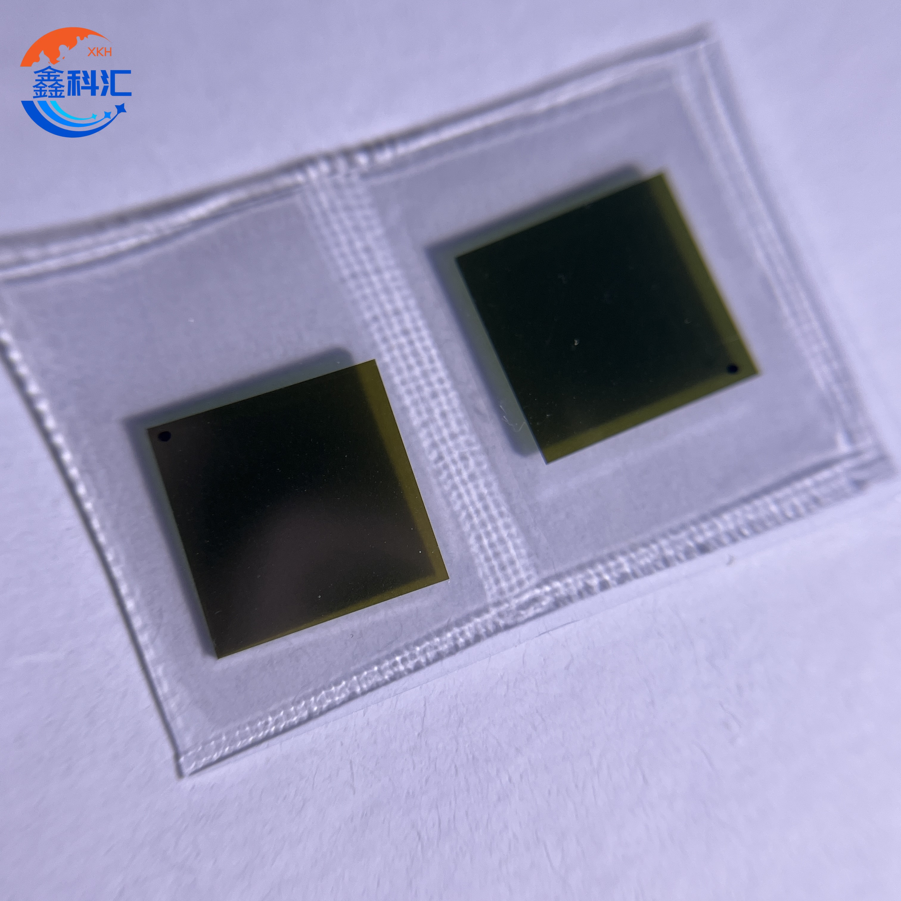
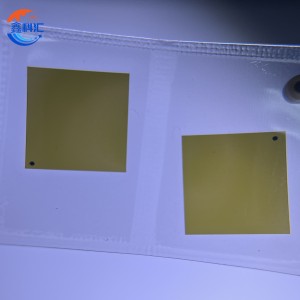
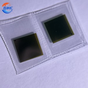
Silicon Carbide (SiC) Single-Crystal Substrate – 10×10mm Wafer


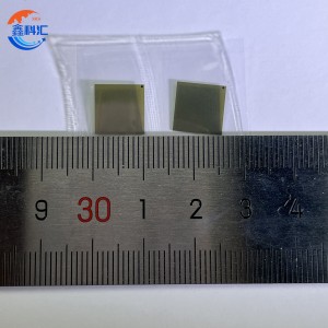
Detailed Diagram of Silicon Carbide (SiC) substrate wafer
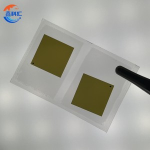
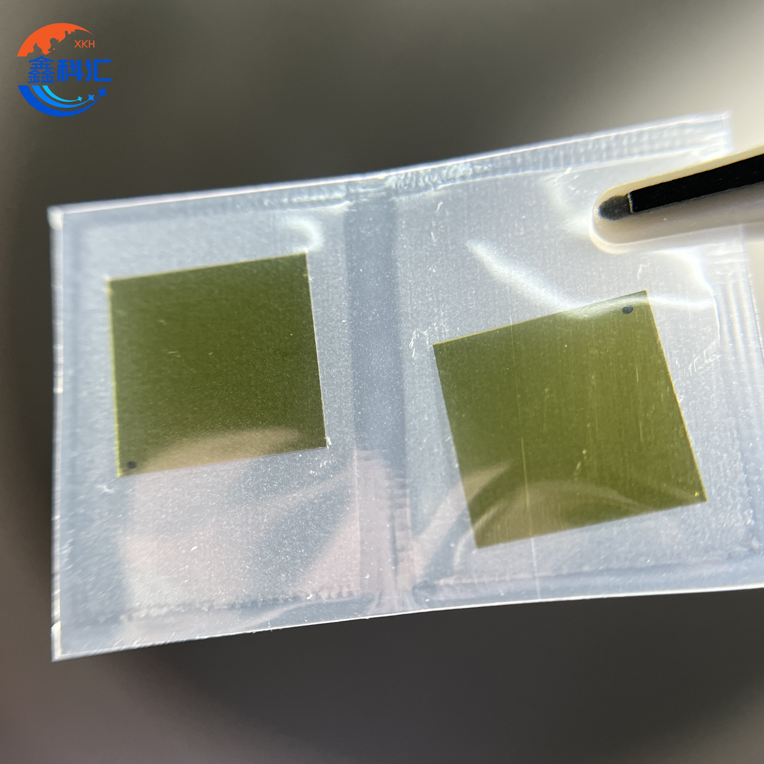
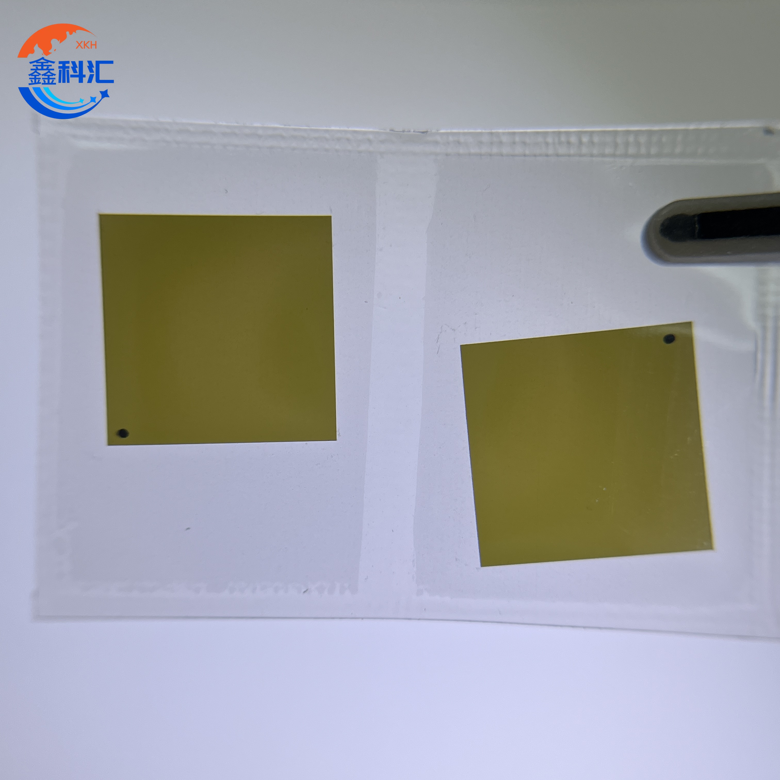
Overview of Silicon Carbide (SiC) substrate wafer
The 10×10mm Silicon Carbide (SiC) single-crystal substrate wafer is a high-performance semiconductor material designed for next-generation power electronics and optoelectronic applications. Featuring exceptional thermal conductivity, wide bandgap, and excellent chemical stability, Silicon Carbide (SiC) substrate wafer provide the foundation for devices that operate efficiently under high temperature, high frequency, and high voltage conditions. These substrates are precision-cut into 10×10mm square chips, ideal for research, prototyping, and device fabrication.
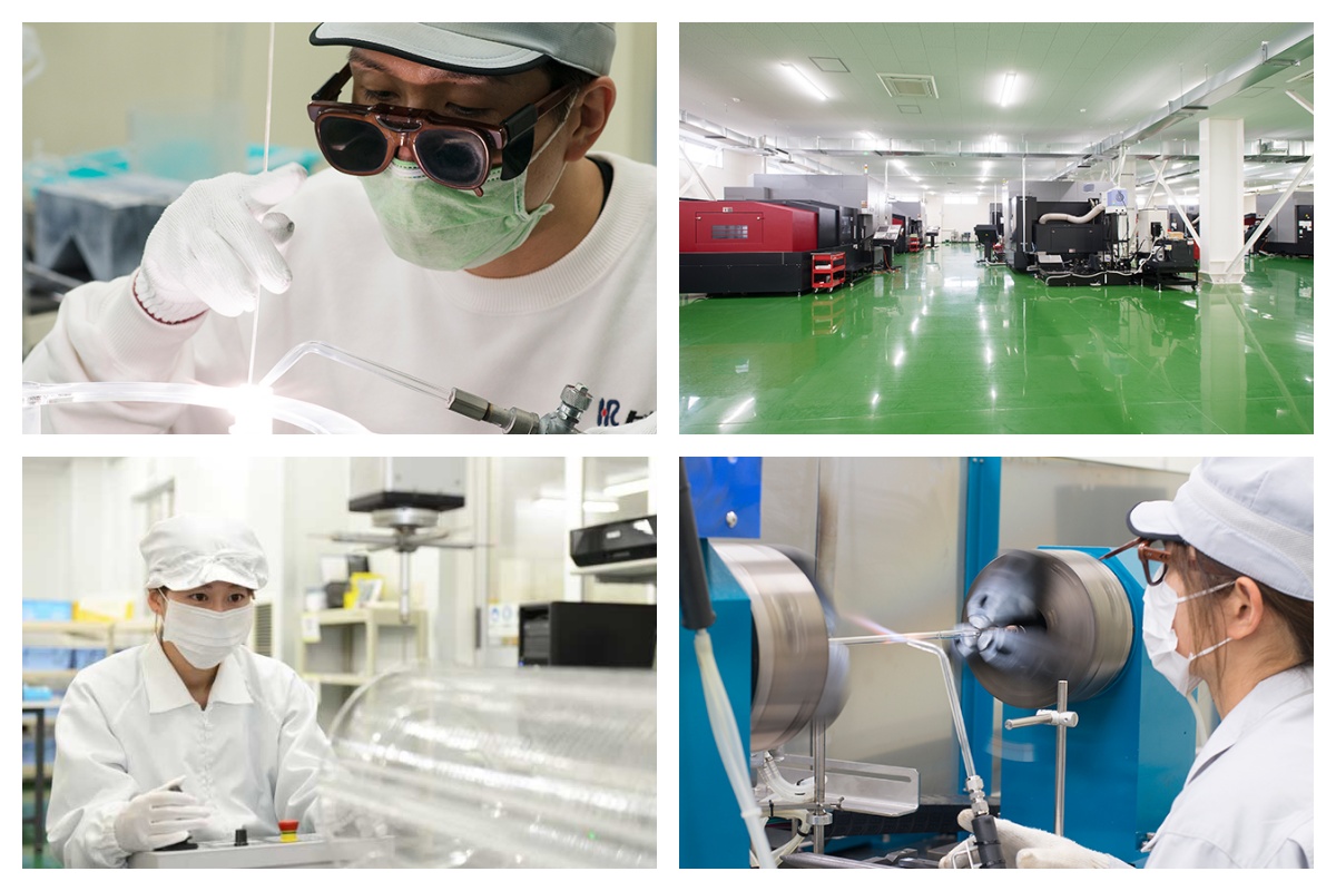
Production Principle of Silicon Carbide (SiC) substrate wafer
Silicon Carbide (SiC) substrate wafer are manufactured through Physical Vapor Transport (PVT) or sublimation growth methods. The process begins with high-purity SiC powder loaded into a graphite crucible. Under extreme temperatures exceeding 2,000°C and a controlled environment, the powder sublimates into vapor and re-deposits onto a carefully oriented seed crystal, forming a large, defect-minimized single crystal ingot.
Once the SiC boule is grown, it undergoes:
- Ingot slicing: Precision diamond wire saws cut the SiC ingot into wafers or chips.
- Lapping and grinding: Surfaces are flattened to remove saw marks and achieve a uniform thickness.
- Chemical Mechanical Polishing (CMP): Achieves an epi-ready mirror finish with extremely low surface roughness.
- Optional doping: Nitrogen, aluminum, or boron doping can be introduced to tailor the electrical properties (n-type or p-type).
- Quality inspection: Advanced metrology ensures wafer flatness, thickness uniformity, and defect density meet stringent semiconductor-grade requirements.
This multi-step process results in robust 10×10mm Silicon Carbide (SiC) substrate wafer chips that are ready for epitaxial growth or direct device fabrication.
Material Characteristics of Silicon Carbide (SiC) substrate wafer
The Silicon Carbide (SiC) substrate wafer are primarily made of 4H-SiC or 6H-SiC polytypes:
-
4H-SiC: Features high electron mobility, making it ideal for power devices such as MOSFETs and Schottky diodes.
-
6H-SiC: Offers unique properties for RF and optoelectronic components.
Key physical properties of Silicon Carbide (SiC) substrate wafer:
-
Wide bandgap: ~3.26 eV (4H-SiC) – enables high breakdown voltage and low switching losses.
-
Thermal conductivity: 3–4.9 W/cm·K – dissipates heat effectively, ensuring stability in high-power systems.
-
Hardness: ~9.2 on Mohs scale – ensures mechanical durability during processing and device operation.
Applications of Silicon Carbide (SiC) substrate wafer
The versatility of Silicon Carbide (SiC) substrate wafer makes them valuable across multiple industries:
Power Electronics: Basis for MOSFETs, IGBTs, and Schottky diodes used in electric vehicles (EVs), industrial power supplies, and renewable energy inverters.
RF & Microwave Devices: Supports transistors, amplifiers, and radar components for 5G, satellite, and defense applications.
Optoelectronics: Used in UV LEDs, photodetectors, and laser diodes where high UV transparency and stability are critical.
Aerospace & Defense: Reliable substrate for high-temperature, radiation-hardened electronics.
Research Institutions & Universities: Ideal for material science studies, prototype device development, and testing new epitaxial processes.

Specifications for Silicon Carbide (SiC) substrate wafer Chips
| Property | Value |
|---|---|
| Size | 10mm × 10mm square |
| Thickness | 330–500 μm (customizable) |
| Polytype | 4H-SiC or 6H-SiC |
| Orientation | C-plane, off-axis (0°/4°) |
| Surface Finish | Single-side or double-side polished; epi-ready available |
| Doping Options | N-type or P-type |
| Grade | Research grade or device grade |
FAQ of Silicon Carbide (SiC) substrate wafer
Q1: What makes Silicon Carbide (SiC) substrate wafer superior to traditional silicon wafers?
SiC offers 10× higher breakdown field strength, superior heat resistance, and lower switching losses, making it ideal for high-efficiency, high-power devices that silicon cannot support.
Q2: Can the 10×10mm Silicon Carbide (SiC) substrate wafer be supplied with epitaxial layers?
Yes. We provide epi-ready substrates and can deliver wafers with custom epitaxial layers to meet specific power device or LED manufacturing needs.
Q3: Are custom sizes and doping levels available?
Absolutely. While 10×10mm chips are standard for research and device sampling, custom dimensions, thicknesses, and doping profiles are available upon request.
Q4: How durable are these wafers in extreme environments?
SiC maintains structural integrity and electrical performance above 600°C and under high radiation, making it ideal for aerospace and military-grade electronics.
About Us
XKH specializes in high-tech development, production, and sales of special optical glass and new crystal materials. Our products serve optical electronics, consumer electronics, and the military. We offer Sapphire optical components, mobile phone lens covers, Ceramics, LT, Silicon Carbide SIC, Quartz, and semiconductor crystal wafers. With skilled expertise and cutting-edge equipment, we excel in non-standard product processing, aiming to be a leading optoelectronic materials high-tech enterprise.
Related Products
-
Custom square box transport box square window p...
-

Lens Prism Optical Glass DSP Custom Size 99.999...
-

SiC ceramic end effector handing arm for wafer ...
-

Silicon carbide ceramic tray sucker Silicon car...
-

Customized SiC Seed Crystal Substrates Dia 205/...
-

Laser Anti-Counterfeiting Marking System for Sa...