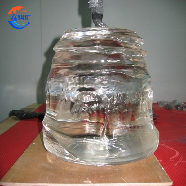
Sapphire Ingot Growth Equipment Czochralski CZ Method for Producing 2inch-12inch Sapphire Wafers


Working Principle
The CZ method operates through the following steps:
1. Melting Raw Materials: High-purity Al₂O₃ (purity >99.999%) is melted in an iridium crucible at 2050–2100°C.
2. Seed Crystal Introduction: A seed crystal is lowered into the melt, followed by rapid pulling to form a neck (diameter <1 mm) to eliminate dislocations.
3. Shoulder Formation and Bulk Growth: The pulling speed is reduced to 0.2–1 mm/h, gradually expanding the crystal diameter to the target size (e.g., 4–12 inches).
4. Annealing and Cooling: The crystal is cooled at 0.1–0.5°C/min to minimize thermal stress-induced cracking.
5. Compatible Crystal Types:
Electronic Grade: Semiconductor substrates (TTV <5 μm)
Optical Grade: UV laser windows (transmittance >90%@200 nm)
Doped Variants: Ruby (Cr³⁺ concentration 0.01–0.5 wt.%), blue sapphire tubing
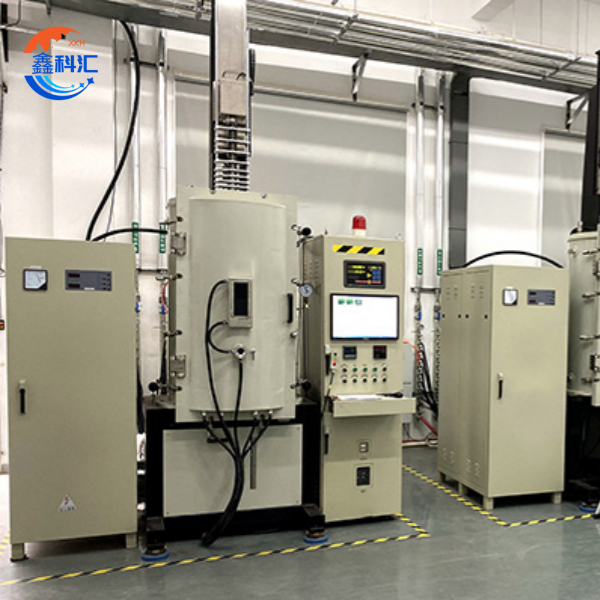
Core System Components
1. Melting System
Iridium Crucible: Resistant to 2300°C, corrosion-resistant, compatible with large melts (100–400 kg).
Induction Heating Furnace: Multi-zone independent temperature control (±0.5°C), optimized thermal gradients.
2. Pulling and Rotation System
High-Precision Servo Motor: Pulling resolution 0.01 mm/h, rotational concentricity <0.01 mm.
Magnetic Fluid Seal: Non-contact transmission for continuous growth (>72 hours).
3. Thermal Control System
PID Closed-Loop Control: Real-time power adjustment (50–200 kW) to stabilize the thermal field.
Inert Gas Protection: Ar/N₂ mixture (99.999% purity) to prevent oxidation.
4. Automation and Monitoring
CCD Diameter Monitoring: Real-time feedback (accuracy ±0.01 mm).
Infrared Thermography: Monitors solid-liquid interface morphology.
CZ vs. KY Method Comparison
| Parameter | CZ Method | KY Method |
| Max. Crystal Size | 12 inches (300 mm) | 400 mm (pear-shaped ingot) |
| Defect Density | <100/cm² | <50/cm² |
| Growth Rate | 0.5–5 mm/h | 0.1–2 mm/h |
| Energy Consumption | 50–80 kWh/kg | 80–120 kWh/kg |
| Applications | LED substrates, GaN epitaxy | Optical windows, large ingots |
| Cost | Moderate (high equipment investment) | High (complex process) |
Key Applications
1. Semiconductor Industry
GaN Epitaxial Substrates: 2–8-inch wafers (TTV <10 μm) for Micro-LEDs and laser diodes.
SOI Wafers: Surface roughness <0.2 nm for 3D-integrated chips.
2. Optoelectronics
UV Laser Windows: Withstand 200 W/cm² power density for lithography optics.
Infrared Components: Absorption coefficient <10⁻³ cm⁻¹ for thermal imaging.
3. Consumer Electronics
Smartphone Camera Covers: Mohs hardness 9, 10× scratch resistance improvement.
Smartwatch Displays: Thickness 0.3–0.5 mm, transmittance >92%.
4. Defense and Aerospace
Nuclear Reactor Windows: Radiation tolerance up to 10¹⁶ n/cm².
High-Power Laser Mirrors: Thermal deformation <λ/20@1064 nm.
XKH's Services
1. Equipment Customization
Scalable Chamber Design: Φ200–400 mm configurations for 2–12-inch wafer production.
Doping Flexibility: Supports rare-earth (Er/Yb) and transition-metal (Ti/Cr) doping for tailored optoelectronic properties.
2. End-to-End Support
Process Optimization: Pre-validated recipes (50+) for LED, RF devices, and radiation-hardened components.
Global Service Network: 24/7 remote diagnostics and on-site maintenance with a 24-month warranty.
3. Downstream Processing
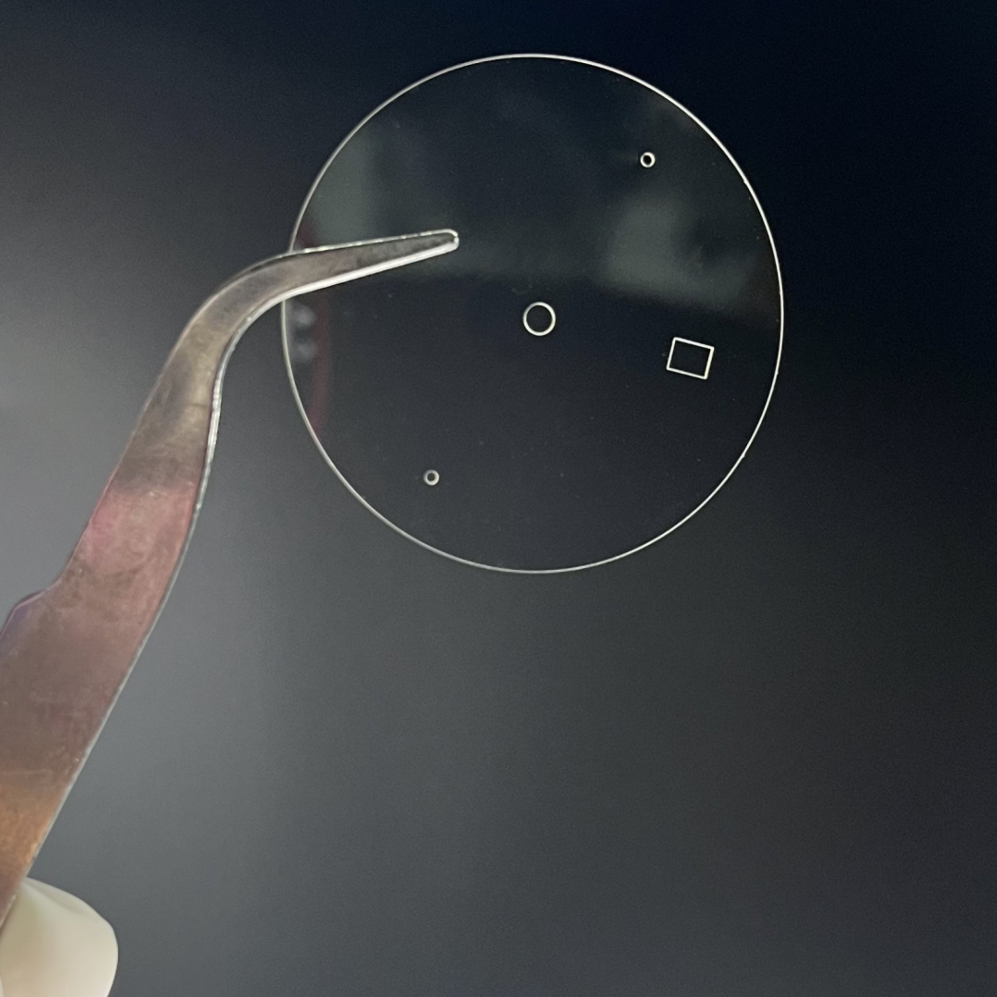
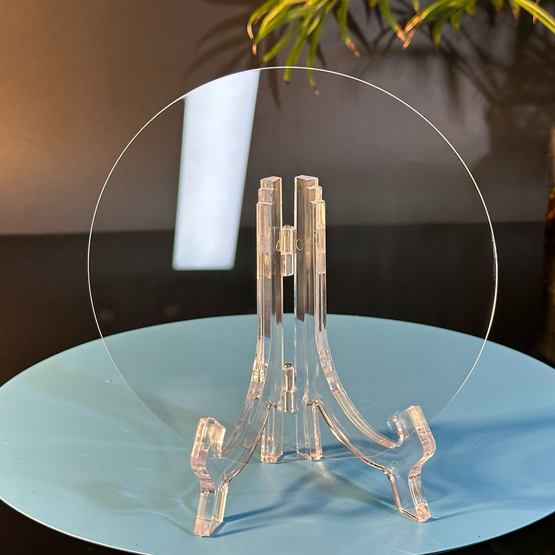
Wafer Fabrication: Slicing, grinding, and polishing for 2–12-inch wafers (C/A-plane).
Value-Added Products:
Optical Components: UV/IR windows (0.5–50 mm thickness).
Jewelry-Grade Materials: Cr³⁺ ruby (GIA-certified), Ti³⁺ star sapphire.
4. Technical Leadership
Certifications: EMI-compliant wafers.
Patents: Core patents in CZ method innovation.
Conclusion
The CZ method equipment delivers large-dimension compatibility, ultra-low defect rates, and high process stability, making it the industry benchmark for LED, semiconductor, and defense applications. XKH provides comprehensive support from equipment deployment to post-growth processing, enabling clients to achieve cost-effective, high-performance sapphire crystal production.