Sapphire Etched Wafer Wet & Dry Etching Solutions


Detailed Diagram


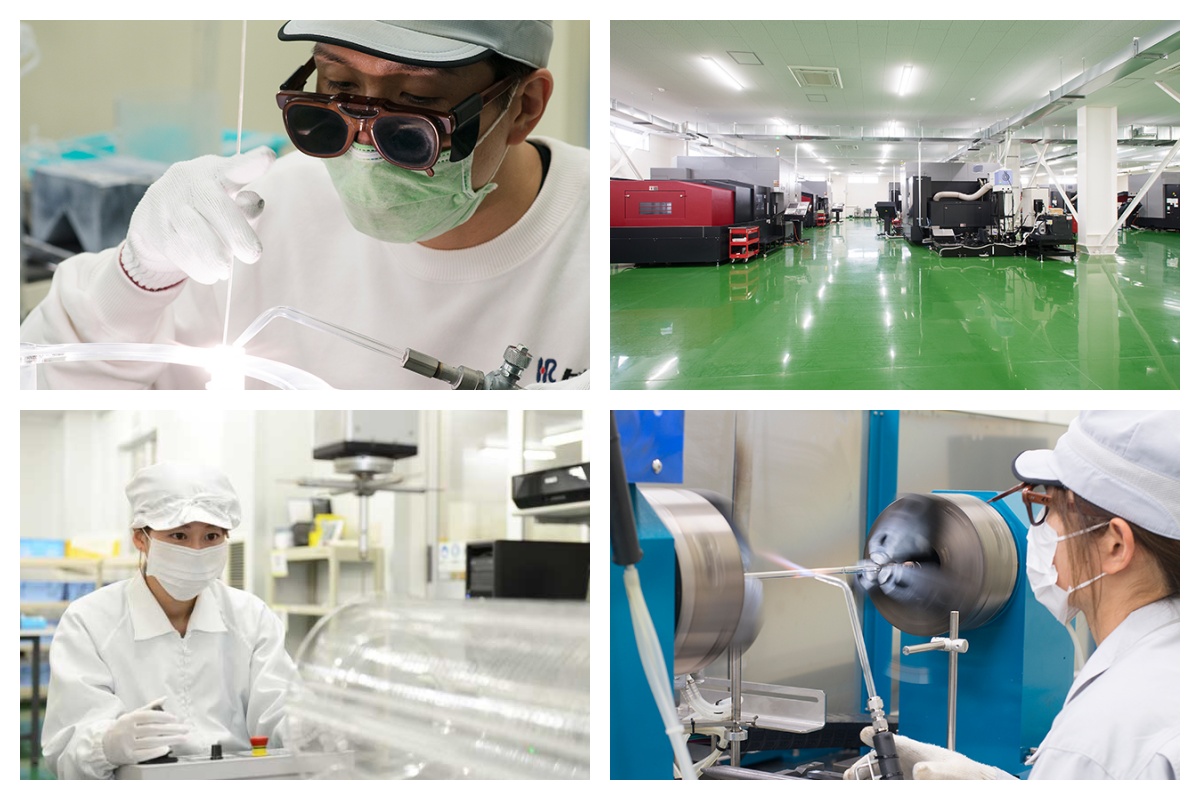
Product Introduction
Sapphire etched wafers are manufactured using high-purity single-crystal sapphire (Al₂O₃) substrates, processed through advanced photolithography combined with wet etching and dry etching technologies. The products feature highly uniform micro-structured patterns, excellent dimensional accuracy, and outstanding physical and chemical stability, making them suitable for high-reliability applications in microelectronics, optoelectronics, semiconductor packaging, and advanced research fields.
Sapphire is well known for its exceptional hardness and structural stability, with a Mohs hardness of 9, second only to diamond. By precisely controlling etching parameters, well-defined and repeatable micro-structures can be formed on the sapphire surface, ensuring sharp pattern edges, stable geometry, and excellent consistency across batches.

Etching Technologies
Wet Etching
Wet etching utilizes specialized chemical solutions to selectively remove sapphire material and form the desired microstructures. This process offers high throughput, good uniformity, and relatively lower processing cost, making it suitable for large-area patterning and applications with moderate sidewall profile requirements.
By accurately controlling solution composition, temperature, and etching time, stable control of etch depth and surface morphology can be achieved. Wet-etched sapphire wafers are widely used in LED packaging substrates, structural support layers, and selected MEMS applications.
Dry Etching
Dry etching, such as plasma etching or reactive ion etching (RIE), employs high-energy ions or reactive species to etch sapphire through physical and chemical mechanisms. This method provides superior anisotropy, high precision, and excellent pattern transfer capability, enabling the fabrication of fine features and high-aspect-ratio microstructures.
Dry etching is particularly suitable for applications requiring vertical sidewalls, sharp feature definition, and tight dimensional control, such as Micro-LED devices, advanced semiconductor packaging, and high-performance MEMS structures.

Key Features and Advantages
-
High-purity single-crystal sapphire substrate with excellent mechanical strength
-
Flexible process options: wet etching or dry etching based on application requirements
-
High hardness and wear resistance for long-term reliability
-
Excellent thermal and chemical stability, suitable for harsh environments
-
High optical transparency and stable dielectric properties
-
High pattern uniformity and batch-to-batch consistency
Applications
-
LED and Micro-LED packaging and testing substrates
-
Semiconductor chip carriers and advanced packaging
-
MEMS sensors and micro-electromechanical systems
-
Optical components and precision alignment structures
-
Research institutes and customized micro-structure development

Customization and Services
We offer comprehensive customization services, including pattern design, etching method selection (wet or dry), etch depth control, substrate thickness and size options, single-side or double-side etching, and surface polishing grades. Strict quality control and inspection procedures ensure that every sapphire etched wafer meets high reliability and performance standards before delivery.
FAQ – Frequently Asked Questions
Q1: What is the difference between wet etching and dry etching for sapphire?
A: Wet etching is based on chemical reactions and is suitable for large-area and cost-effective processing, while dry etching uses plasma or ion-based techniques to achieve higher precision, better anisotropy, and finer feature control. The choice depends on structural complexity, precision requirements, and cost considerations.
Q2: Which etching process should I choose for my application?
A: Wet etching is recommended for applications requiring uniform patterns with moderate accuracy, such as standard LED substrates. Dry etching is more suitable for high-resolution, high-aspect-ratio, or Micro-LED and MEMS applications where precise geometry is critical.
Q3: Can you support customized patterns and specifications?
A: Yes. We support fully customized designs, including pattern layout, feature size, etch depth, wafer thickness, and substrate dimensions.
About Us
XKH specializes in high-tech development, production, and sales of special optical glass and new crystal materials. Our products serve optical electronics, consumer electronics, and the military. We offer Sapphire optical components, mobile phone lens covers, Ceramics, LT, Silicon Carbide SIC, Quartz, and semiconductor crystal wafers. With skilled expertise and cutting-edge equipment, we excel in non-standard product processing, aiming to be a leading optoelectronic materials high-tech enterprise.