Sapphire Crystal Growth Furnace KY Kyropoulos Method for Sapphire Wafer and Optical Window Production


Working Principle
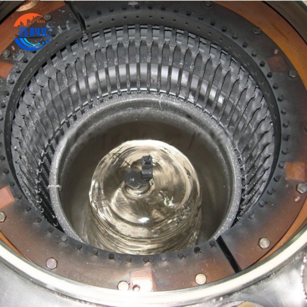
The core principle of the KY method involves melting high-purity Al₂O₃ raw materials in a tungsten/molybdenum crucible at 2050°C. A seed crystal is lowered into the melt, followed by controlled withdrawal (0.5–10 mm/h) and rotation (0.5–20 rpm) to achieve directional growth of α-Al₂O₃ single crystals. Key features include:
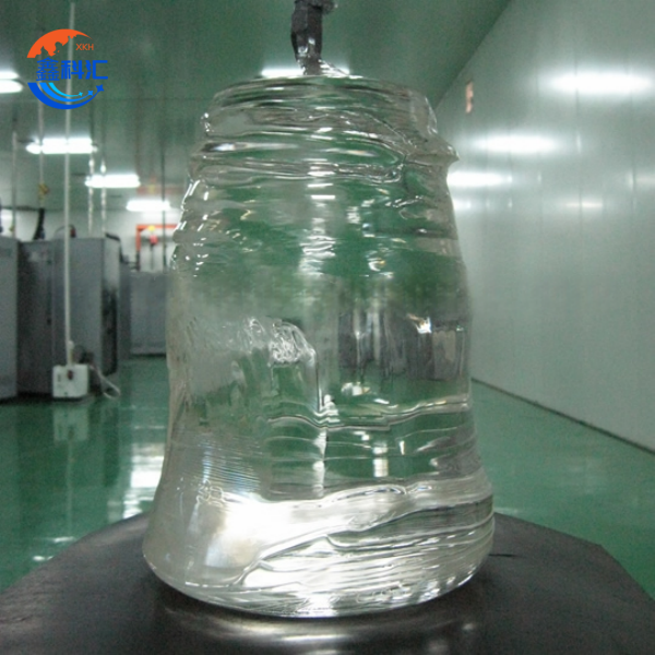
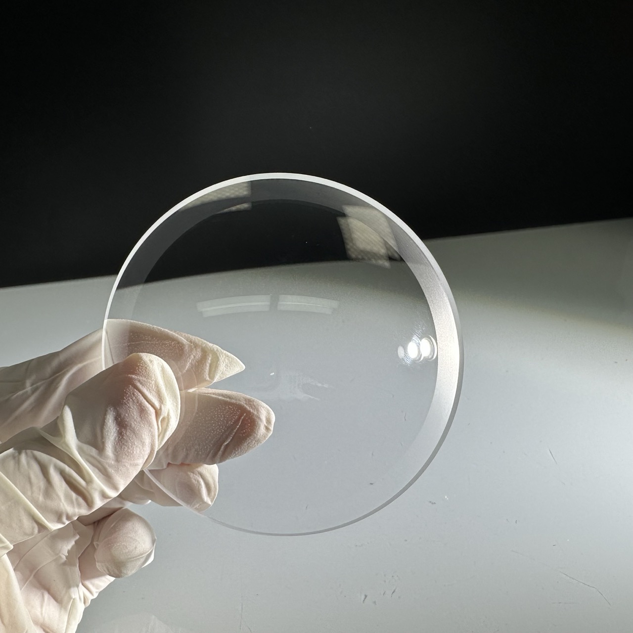
• Large-dimension crystals (max. Φ400 mm × 500 mm)
• Low-stress optical-grade sapphire (wavefront distortion <λ/8 @ 633 nm)
• Doped crystals (e.g., Ti³⁰ doping for star sapphire)
Core System Components
1. High-Temperature Melting System
• Tungsten-molybdenum composite crucible (max. temp. 2300°C)
• Multi-zone graphite heater (±0.5°C temperature control)
2. Crystal Growth System
• Servo-driven pulling mechanism (±0.01 mm precision)
• Magnetic fluid rotary seal (0–30 rpm stepless speed regulation)
3. Thermal Field Control
• 5-zone independent temperature control (1800–2200°C)
• Adjustable heat shield (±2°C/cm gradient)
• Vacuum & Atmosphere System
• 10⁻⁴ Pa high vacuum
• Ar/N₂/H₂ mixed gas control
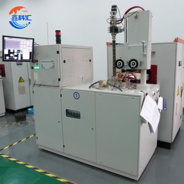
4. Intelligent Monitoring
• CCD real-time crystal diameter monitoring
• Multi-spectral melt level detection
KY vs. CZ Method Comparison
| Parameter | KY Method | CZ Method |
| Max. Crystal Size | Φ400 mm | Φ200 mm |
| Growth Rate | 5–15 mm/h | 20–50 mm/h |
| Defect Density | <100/cm² | 500–1000/cm² |
| Energy Consumption | 80–120 kWh/kg | 50–80 kWh/kg |
| Typical Applications | Optical windows/large wafers | LED substrates/jewelry |
Key Applications
1. Optoelectronic Windows
• Military IR domes (transmittance >85%@3–5 μm)
• UV laser windows (withstand 200 W/cm² power density)
2. Semiconductor Substrates
• GaN epitaxial wafers (2–8 inch, TTV <10 μm)
• SOI substrates (surface roughness <0.2 nm)
3. Consumer Electronics
• Smartphone camera cover glass (Mohs hardness 9)
• Smartwatch displays (10× scratch resistance improvement)
4. Specialized Materials
• High-purity IR optics (absorption coefficient <10⁻³ cm⁻¹)
• Nuclear reactor observation windows (radiation tolerance: 10¹⁶ n/cm²)
Advantages of Kyropoulos (KY) Sapphire Crystal Growth Equipment
The Kyropoulos (KY) method-based sapphire crystal growth equipment offers unparalleled technical advantages, positioning it as a cutting-edge solution for industrial-scale production. Key benefits include:
1. Large-Diameter Capability: Capable of growing sapphire crystals up to 12 inches (300 mm) in diameter, enabling high-yield production of wafers and optical components for advanced applications such as GaN epitaxy and military-grade windows.
2. Ultra-Low Defect Density: Achieves dislocation densities <100/cm² through optimized thermal field design and precise temperature gradient control, ensuring superior crystal integrity for optoelectronic devices.
3. High-Quality Optical Performance: Delivers transmittance >85% across visible to infrared spectra (400–5500 nm), critical for UV laser windows and infrared optics.
4. Advanced Automation: Features servo-driven pulling mechanisms (±0.01 mm precision) and magnetic fluid rotary seals (0–30 rpm stepless control), minimizing human intervention and enhancing consistency.
5. Flexible Doping Options: Supports customization with dopants like Cr³⁰ (for ruby) and Ti³⁰ (for star sapphire), catering to niche markets in optoelectronics and jewelry.
6. Energy Efficiency: Optimized thermal insulation (tungsten-molybdenum crucible) reduces energy consumption to 80–120 kWh/kg, competitive with alternative growth methods.
7. Scalable Production: Achieves a monthly output of 5,000+ wafers with rapid cycle times (8–10 days for 30–40 kg crystals), validated by over 200 global installations.
8. Military-Grade Durability: Incorporates radiation-resistant designs and heat-resistant materials (withstand 10¹⁶ n/cm²), essential for aerospace and nuclear applications.
These innovations solidify the KY method as the gold standard for producing high-performance sapphire crystals, driving advancements in 5G communications, quantum computing, and defense technologies.
XKH Services
XKH provides comprehensive turnkey solutions for sapphire crystal growth systems, encompassing installation, process optimization, and staff training to ensure seamless operational integration. We deliver pre-validated growth recipes (50+) tailored to diverse industrial needs, significantly reducing R&D time for clients. For specialized applications, custom development services enable cavity customization (Φ200–400 mm) and advanced doping systems (Cr/Ti/Ni), supporting high-performance optical components and radiation-resistant materials.
Value-added services include post-growth processing such as slicing, grinding, and polishing, complemented by a full range of sapphire products like wafers, tubes, and gemstone blanks. These offerings cater to sectors from consumer electronics to aerospace. Our technical support guarantees a 24-month warranty and real-time remote diagnostics,ensuring minimal downtime and sustained production efficiency.
Related Products
-

SiC Ingot 4H type Dia 4inch 6inch Thickness 5-1...
-
SiC ceramic tray plate graphite with CVD SiC co...
-

SiC ceramic plate/tray for 4inch 6inch wafer ho...
-
Sapphire dome transparent High hardness 9.0 res...
-

4H-N/6H-N SiC Wafer Reasearch production Dummy ...
-

P-type SiC wafer 4H/6H-P 3C-N 6inch thickeness...