Precision Microjet Laser System for Hard & Brittle Materials


Key Features
1. Dual-Wavelength Nd:YAG Laser Source
Utilizing a diode-pumped solid-state Nd:YAG laser, the system supports both green (532nm) and infrared (1064nm) wavelengths. This dual-band capability enables superior compatibility with a wide spectrum of material absorption profiles, improving processing speed and quality.
2. Innovative Microjet Laser Transmission
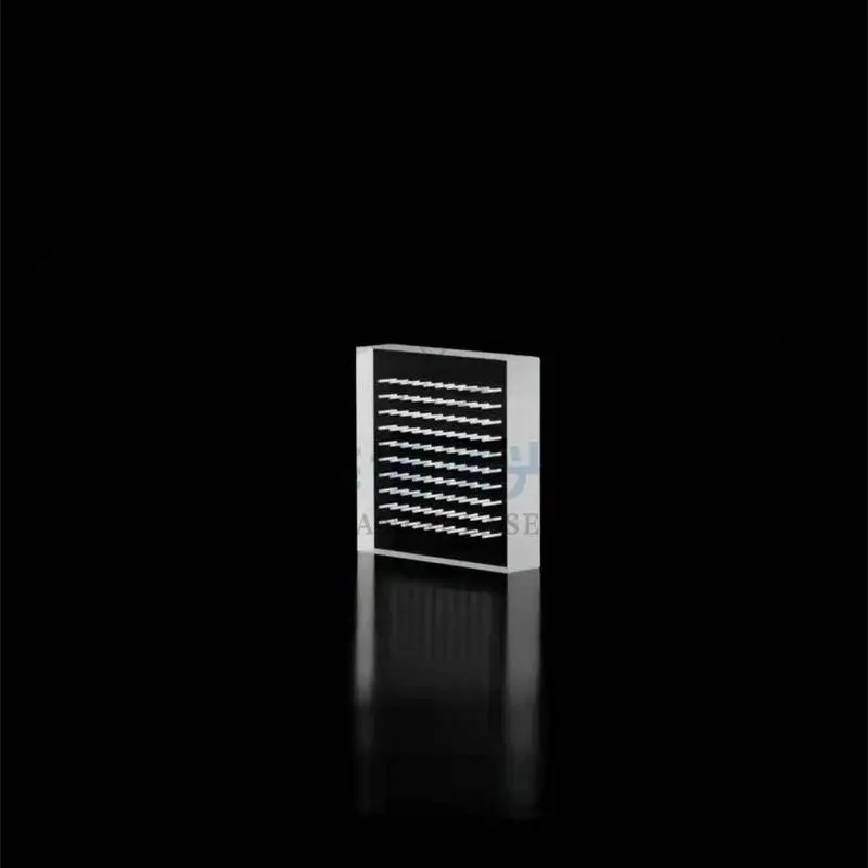
By coupling the laser with a high-pressure water microjet, this system exploits total internal reflection to channel laser energy precisely along the water stream. This unique delivery mechanism ensures ultra-fine focus with minimal scattering and delivers line widths as fine as 20μm, offering unmatched cut quality.
3. Thermal Control at Micro Scale
An integrated precision water-cooling module regulates temperature at the processing point, maintaining the heat-affected zone (HAZ) within 5μm. This feature is especially valuable when working with heat-sensitive and fracture-prone materials such as SiC or GaN.
4. Modular Power Configuration
The platform supports three laser power options—50W, 100W, and 200W—allowing customers to select the configuration that matches their throughput and resolution requirements.
5. Precision Motion Control Platform
The system incorporates a high-accuracy stage with ±5μm positioning, featuring 5-axis motion and optional linear or direct-drive motors. This ensures high repeatability and flexibility, even for complex geometries or batch processing.
Application Areas
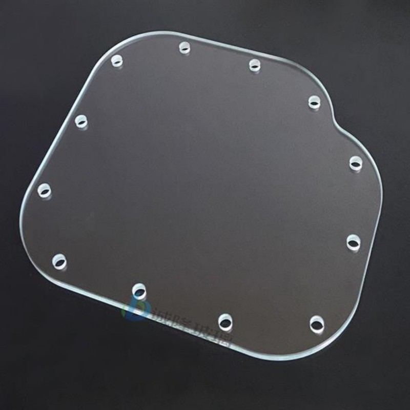
Silicon Carbide Wafer Processing:
Ideal for edge trimming, slicing, and dicing of SiC wafers in power electronics.
Gallium Nitride (GaN) Substrate Machining:
Supports high-precision scribing and cutting, tailored for RF and LED applications.
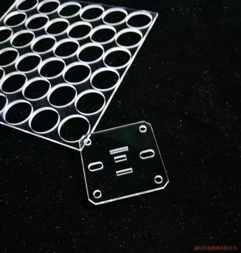
Wide Bandgap Semiconductor Structuring:
Compatible with diamond, gallium oxide, and other emerging materials for high-frequency, high-voltage applications.
Aerospace Composite Cutting:
Precise cutting of ceramic matrix composites and advanced aerospace-grade substrates.
LTCC & Photovoltaic Materials:
Used for micro via drilling, trenching, and scribing in high-frequency PCB and solar cell manufacturing.
Scintillator & Optical Crystal Shaping:
Enables low-defect cutting of yttrium-aluminum garnet, LSO, BGO, and other precision optics.
Specification
|
Specification |
Value |
| Laser Type | DPSS Nd:YAG |
| Wavelengths Supported | 532nm / 1064nm |
| Power Options | 50W / 100W / 200W |
| Positioning Accuracy | ±5μm |
| Minimum Line Width | ≤20μm |
| Heat-Affected Zone | ≤5μm |
| Motion System | Linear / Direct-drive motor |
| Max Energy Density | Up to 10⁷ W/cm² |
Conclusion
This microjet laser system redefines the limits of laser machining for hard, brittle, and thermally sensitive materials. Through its unique laser-water integration, dual-wavelength compatibility, and flexible motion system, it offers a tailored solution for researchers, manufacturers, and system integrators working with cutting-edge materials. Whether used in semiconductor fabs, aerospace labs, or solar panel production, this platform delivers reliability, repeatability, and precision that empower next-generation material processing.
Detailed Diagram
Related Products
-

Gold Coated Silicon Wafers 2inch 4inch 6inch Go...
-

Al2O3 99.999% sapphire custom blade transparent...
-

Sapphire Tube Unpolished Small Size Al2O3 Glass...
-

SiC Ingot 4H-N type Dummy grade 2inch 3inch 4in...
-
Transparent sapphire tubes pipes rods high temp...
-

LiTaO3 Lithium Tantalate Ingots with Fe/Mg Dopi...